From the microcontroller to ARM, the main need to learn ARM architecture, ARM compared to the microcontroller has some peripherals and bus. In the case of just streaking, if you are familiar with the ARM architecture, then I think there will be no difference between using any ARM architecture chip and using the microcontroller. The reason why the ARM architecture is more complex is of course to run faster and better support system-on-chip, so to a certain extent, if the on-chip system is not well understood, then the understanding of ARM architecture will not be so deep.
This article first introduces the ARM architecture diagram and various modes. Secondly, it introduces general registers, basic concepts of MMU related addresses, and three types of addresses in ARM920T. Finally, the ARM processor architecture and naming rules are described.
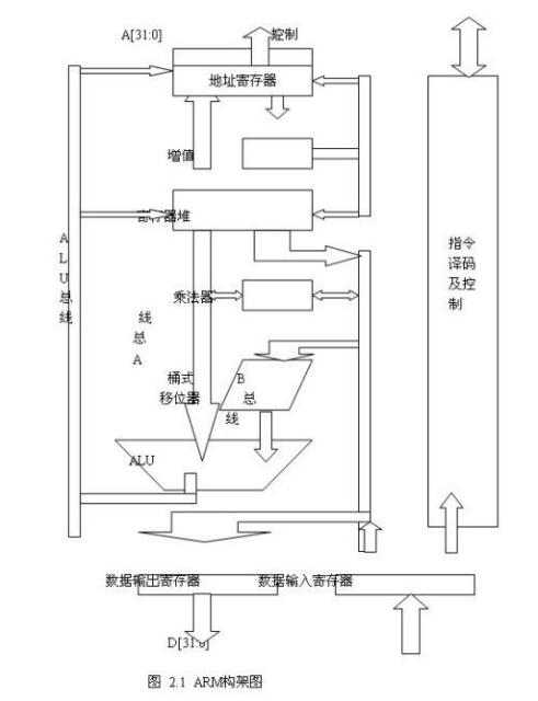
First, ARM architecture diagramThe following figure shows the ARM architecture diagram. It consists of a 32-bit ALU, several 32-bit general-purpose registers and status registers, 32 & TImes; 8-bit multipliers, 32 & TImes; 32-bit barrel shifter, instruction decode and control logic, instruction pipeline, and data/address registers.
1.ALU: It consists of two operand latches, adders, logic functions, results, and zero detect logic.
2. Barrel shift register: ARM uses 32 & TImes; 32-bit barrel shifter, which can make the left shift / right shift n bits, loop shift n bits and arithmetic shift right n bits can be completed at once.
3. High-speed multipliers: Multipliers generally use the "plus one shift" method to achieve multiplication. In order to improve the computing speed, ARM uses a two-multiply method to implement “add-shift†operations based on the 2 bits of the multiplier. The ARM high-speed multiplier uses a 32-bit TIMER 8-bit structure so that the integration can be reduced. The corresponding chip area is less than 1/3 of the parallel multiplier.
4. Floating-point components: Floating-point components are used as an option for ARM architectures. The FPA10 floating-point accelerator is connected to the ARM as a co-processing method and executed through the interpretation of the co-processing instructions.
5. Controller: The ARM controller uses a hard-wired programmable logic array PLA.
6. Registers
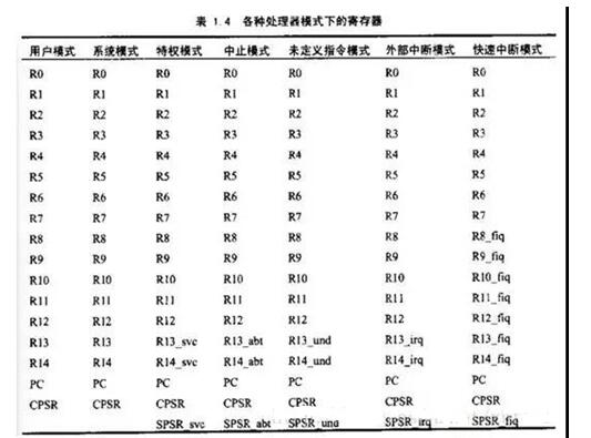
ARM has the following 7 modes:
User mode (user,usr) Mode of normal program execution
Fast Interrupt Mode (FIQ,fiq) for high-speed data transmission and channel processing
External interrupt mode (IRQ, irq) for normal interrupt handling
Supervisor (svc) A protection mode used by the operating system
Data Abort Mode (Abort, abt) for Virtual Storage and Storage Protection
Undefined (und defined) mode is used to support coprocessors via software guidelines
System mode (System, sys) is used to run privileged operating system tasks
In addition to the user mode, they are called privileged modes. In privileged modes, except for the system mode, they are called exception modes, ie exception mode. My understanding of the word "abnormality" at first was somewhat biased. I think the abnormal pattern is that this system has made a mistake, but it is not. The meaning of the exception mode is an exception, meaning "when this mode happens, it doesn't say...", for example, an external interrupt will also enter the abnormal mode, but at this time the system is running perfectly.
Among them SVC is used in the boot file BOOT program that the system just started, must be SVC before jumping to kernel, SVC has the highest authority, can operate on any register. In bare metal programs we sometimes stay in SVC mode.
When it comes to user mode or system mode, the following is my guess, such as entering the linux kernel will be set to sys mode, such as task scheduling, etc. will be in sys mode, and the implementation of user-written applications, the system is In usr mode. The above guesses need to find evidence verification in linux.
Among them, FIQ and IRQ are interrupt modes. When an interrupt occurs, it will enter FIQ mode or IRQ mode. As for which mode is entered, it is set by the developer. In theory, the response speed of the FIQ mode is faster than that of the IRQ mode.
The abt mode usually occurs when the access address is not aligned. At this time, it will jump to the interrupt vector address to which abt belongs. Und mode should be found after the instruction to find the instruction can not be used, at this point will jump to abt belongs to the interrupt vector address. The above two modes should be entered during the development process, and it is also a debugging method. These errors should be eliminated before the release of the version.
Third, the general registerR13 is usually used as a stack pointer. When entering the exception mode, the register to be used can be saved in the stack pointed to by R13. When exiting the abnormal blowing program, the register value stored in the stack pointed to by R13 is popped up.
R14 is also called the Link Register (LR), which is the PC's return value.
R15 is also recorded as a PC. The ARM instructions are word-aligned and the 0th and 1st bits of the PC's value are always 0. That is 32-bit alignment.
For the Cortex-M3, there is a register bank with R0-R15. Where R13 acts as a stack pointer SP. There are two SPs, R13 (MSP) and R13 (PSP), the main stack pointer (MSP) and the process stack pointer (PSP), but only one can be seen at the same time. This is called "banked." "register. These registers are 32-bit.
Fourth, the basic concept of MMU related addressRegarding the MMU, because of the different physical addresses and inconsistencies of various storage devices, it is necessary to place the addresses on a reasonable continuous virtual address, so the MMU appears. The MMU places different addresses in suitable virtual addresses for scheduling. For example, to run LINUX must have MMU support.
Five, there are three types of addresses in ARM920TVirtual Address (VA), Transformed Virtual Address (MVA), Physical Address (PA).
Here is an example of what an address does when an instruction is requested:
1. Instruction VA (IVA) issued by ARM920T
2. It is converted into the instruction MVA (IMVA) by the ProcID (number of the process space block where the current process is located). The instruction CACHE (ICACHE) and the MMU see the IMVA.
3. If the protection module on the IMMU confirms that IMVA will not be interrupted and the IMVA tag is also in ICACHE, the instruction data will be read out and returned to the ARM920T core.
4. If the IMVA tag is not in ICACHE, the IMMU will generate a command PA (IPA). The address will give the AMBA bus interface to get external data.
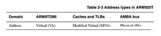
So how is VA converted from PID to MVA?
This is about 13 in FC15, FCSE PID register
R13 is the fast context switch extension process identifier. This register is reset to zero.
Reading R13 will get the FCSE PID value. Writing R13 updates the FCSE PID value to [31:25]. Bits [24:0] should be zero.
How to use FCSE PID:
The addresses issued by the 920T kernel are all in the range of 0-32 MB. The reverse-order space of 4 GB is divided into 1238 process space blocks, and the size of each process space block is 32 MB. Each process space block can contain one process. The system actually uses the virtual address space of the processes in the process space block numbered from 0 to 127 of the 128 process space blocks (I*0x02000000) to (I*0x02000000+0x01FFFFFF).
So VA is usually 0 when all 7 are 0 MVA = VA | (PID "" 25)
When the VA high 7 bits are not 0, MVA = VA, this VA is a virtual address used by the process to access data and instructions in other processes. Note that the process identifier being accessed cannot be 0 at this time.
Note: When the FCSE_PID is 0, that is, the current reset, the current 920T and CACHES and MMU is a plane mapping relationship (very clever:)).
What is TLB?TLB translate look-aside buffer, fast table is to store several commonly used page tables, in order to improve the speed of the system. Before updating the page table, it must be invalidated. The register for its operation is R8. R8 is a write-only register, and reading it will cause incalculable consequences.
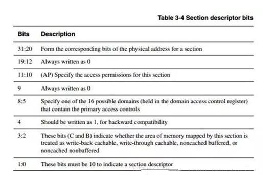
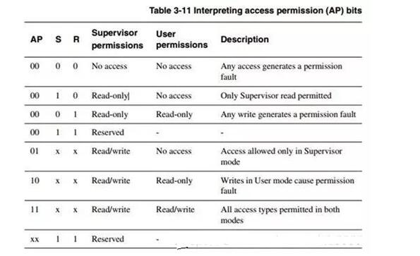
The DOMAIN assignment is in C3, 32bit total 16 domains, each domain is divided into two bits, these two bits control the current domain permissions. The above four bits are for selecting one of 0-15 domains.
Eight, on the C, B assignment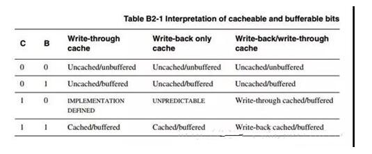
The above is about two kinds of write cache, write and write back. The write back method refers to that when the CPU performs a write operation, the written data is only written into the cache, and is not written into the main memory. Only when it needs to be replaced, the cached block that has been modified is written back to the main memory. Write-through means that the CPU must write data to the cache and main memory at the same time when performing a write operation.
Nine, clock and bus conceptFCLK, HCLK, andPCLK
FCLK is used byARM920T.
HCLK is used for the AHB bus, which is used by the ARM920T, the memory controller, the interrupt controller, the LCD controller, the DMA and USB host block.
PCLK is used for APB bus, which is used by the peripherals such as WDT, IIS, I2C, PWM timer, MMC interface, ADC, UART, GPIO, RTC and SPI.
What is AHB/APB?
The InternalAdvanced Microcontroller Bus Architecture (AMBA) is a bus standard and both of the following are in compliance with this standard.
AHB (Advanced High Performance Bus) is mainly used for system high-performance, high-speed rate module communication.
APB (Advanced Peripheral Bus) is mainly used for communication between slow on-chip peripherals and the ARM core.
The AHB Private Peripheral Bus is used only for the AHB peripherals inside the CM3. These are: NVIC, FPB, DWT and ITM.
The APB Private Peripheral Bus is used both for APB devices inside the CM3 and for external devices (the “external†here is for the kernel). CM3 allows device manufacturers to add some on-chip APB peripherals to the APB private bus, which are accessed through the APB interface.
Ten or four power consumption modesNORMAL, SLOW, IDLE, SLEEP
First configure the main PLL MPLL for the CPU. The PLL is unstable during a power-on reset, so Fin skips MP11 directly to FCLK before PLLCON is configured by software, so configuring PLLCON is also fine. Even under normal operation, the MPLLCON can be configured. After the configuration, the CLKs of the internal modules can be normally supplied after waiting for the PLL lock-time.
Eleven, arm processor architecture explainWhat about the architecture? Look at a picture again.
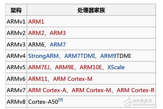
The left side is the architecture, the right side is the processor, and it can also be called the core. The arm's first successful CPU is the ARM7TDMI, which is based on ARMv4. The ARM architecture includes the following RISC features:
Read/store architecture
Address unaligned memory access is not supported (ARMv6 core is now supported)
Orthogonal instruction set (arbitrary access instructions can access data in any addressing mode Orthogonal instrucTIon set)
A large number of 16 & TImes; 32-bit register files
The fixed 32-bit opcode length reduces the amount of code generated and reduces the burden of decoding and pipelining.
Most of them are executed in one CPU cycle.
Different versions of the architecture will be adjusted.
The other major companies that cooperate with ARM, like Samsung, usually put their CPUs and various peripheral IPs together. Then they take their own drawings to stream. They produce a square, with many pins underneath. This thing contains not only the CPU, but also other controllers. This thing is called SOC (system on chip). From an English perspective, the so-called quad-core SOC is not intended to refer to the CPU alone but to the quad-core system.
So what the major manufacturers do now is to buy the ARM license and get the source code of the ARM processor, and then engage in some external IP (or buy or design) to form a SOC and then stream it out. Different SOCs have different architectures (that is, how CPUs relate to IP, some use buses as the core, and some use DDR as the core). Therefore, Hass is an SOC architecture with independent property rights. However, no matter how many manufacturers, no matter how toss, have not moved CPU, ARM core just stay there, it is the central processor.
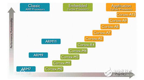
Current ARM product ladders:
ARM naming rules:
First figure: Series name: eg.ARM7, ARM9
The second number: Memory system
2: With MMU
4: With MPU
6: No MMU and MPU
The third number: Memory size
0: Standard Cache (4-128k)
2: Reduced Cache
6: Variable Cache
The fourth character: T: indicates that the Thumb instruction set is supported
D: indicates support for on-chip debugging (Debug)
M: indicates an embedded hardware multiplier (MulTIplier)
I : Supports on-chip breakpoints and debug points
E: indicates support for enhanced DSP functions
J: Express support for Jazelle technology, Java accelerator
S: Fully synthetic
If you are tired of the original back of your phone, you should try our 3D Relief Back Sticker. The Back Skin Protective Film on the back can not only bring you a visual change, but also protect the back cover of the phone itself from scratches and collisions. Real 3D touch, personalized and stylish pattern design. Bring you a perfect experience.
In daily use, it can protect the equipment from scratches, dust, impact and other damage.
Long-lasting anti-scratch effect, significantly reducing dust, oil stains and fingerprint stains.
Easy to install, easy to stick to the back of the phone, and will not damage the original appearance of the phone.
With the Protective Film Cutting Machine, you can install the Back Film on different types of mobile phone back shells, including mobile phones, tablet computers and other electronic products. Customization can be completed in 30 seconds with just one click.
If you want to know more about 3D Relief Back Sticker, please click product details to view the parameters, models, pictures, prices and other information about 3D Relief Back Sticker.
Whether you are a group or an individual, we will try our best to provide you with accurate and comprehensive information about 3D Relief Back Sticker!
3D Phone Sticker, Carbon Fiber Back Sticker, 3D Relief Back Sticker, 3D Printing Back Sticker, Phone Skin,Mobile Phone Back Sticker
Shenzhen Jianjiantong Technology Co., Ltd. , https://www.tpuscreenprotector.com