This white paper explores the VLFFT demo of the TMS320C6678 processor. The 16K-1024K one-dimensional single-precision floating-point FFT algorithm samples are executed by the TMS320C6678 processor with eight fixed and floating-point DSP cores to detect their respective running times when using 1, 2, 4 or 8 cores. The results of the demonstration demonstrate the superior performance of the C66X DSP core and the fact that the TMS320C6678 processor is proportional to the number of cores across multicore parallelization performance.
The demonstrations herein use the FFT algorithm, which is frequently used in fields such as medical imaging, communications, military and commercial radar, and electronic warfare (jammers, anti-jammers). The results of this paper show that when the operating rate is 1 GHz and the DSP core is 8, it takes only 6.4 milliseconds to execute the 1024K FFT algorithm sample with the TMS320C6678 processor.
TMS320C6678 SoC
The TMS320C6678 processor has eight DSP cores and is based on TI's C66x fixed and floating point DSP cores and TI's innovative KeyStone architecture with multi-core rights. It runs at speeds up to 1.25 GHz, and at this speed it can perform 160 gigaflops per second, and typically consumes less than 10 watts of power. The TMS320C6678 processor features a DSP core. 512KB of L2 memory; in addition, 8MB of chip memory has 4MB of shared memory, and both of these memories have error correction codes. Its DDR3 interface is 64-bit, with 8-bit error correction code, running at speeds of up to 1600 megabits per second, while supporting up to 8GB of external memory data access. In addition, the TMS320C6678's companion peripherals include PCle, Serial RapidIO, Gigabit Ethernet and TI's HyperLink interface, which provides up to 50Gbps connectivity when connected to TI's other DSPs, ARM, ARM+DSP processors and third-party FPGAs. speed.
In the VLFFT demo of this article, the TMS320C6678 processor runs at 1GHz and the DDR3 interface has a transfer speed of 1333MHz.

Figure 1: Block diagram of TMS320C6678
VLFFT demo
Since the VLFFT algorithm requires the input data to be stored in the external memory of the processor, during the demonstration, the data is accessed, allocated, and processed by the DSP core, and the result is finally output to the external memory. At the same time, cycle counts and time measurements are always maintained throughout the process. During the demonstration, the TMS320C6678 processor is configured with a different number of cores (1, 2, 4 or 8) to calculate the results when the FFT size is different. These FFT specifications include: 16K 32K 64K 128K 156K 512K 1024K
During the demonstration, the performance of the FFT was maximized by distributing the computational load across multiple cores and fully utilizing the high-performance computing power of the C66X DSP core. At the same time, the one-dimensional VLFFT algorithm is expressed by a similar two-dimensional FFT algorithm using the basic time extraction algorithm. This method is decomposed into a form of N=N1*N2 when a very large data N is encountered. In the present demonstration, if the one-dimensional input array is very large, it is represented by a two-dimensional array of N1 rows * N2 columns, and then the FFT is calculated by the following steps:
Calculate the FFT of the N2 column array in different sizes in the N1 row array; multiply by the rotation factor; store the result of the FFT algorithm when the N2 column is different in the N1 row, form a two-dimensional array of N2*N1; calculate the N1 row array in N2 The FFT of different sizes in the column array; the data in the storage column direction forms a two-dimensional array of N2*N1.
This algorithm is called high-performance parallel FFT algorithm by Takahashi called Hitachi SR8000.
When performing the multi-core algorithm, the first step is to calculate the FFT algorithm for the N2 column (the number of cores) under the N1 line specification, and the fourth step is to calculate the FFT algorithm for the N1 row (the number of cores) under the N2 column specification. The 0 core is the primary core and is responsible for synchronizing with all remaining affiliate cores. According to the size of the N1 array and the N2 array, the total number of FFTs calculated by each core is divided into several smaller modules to accommodate the space of each core L2 SRAM memory. Each set of data is prefetched into the L2 SRAM memory by DMA in external memory and then returned to the external memory via DDR. Each core uses two DMA channels to convert input and output data in external memory (DDR3) and internal memory (L2 SRAM).
result
Figure 1 on the next page shows the results of the TMS320C6678 evaluation version (TMDSEVM6678LE) running the FFT code in one DSP cycle and one millisecond unit time, respectively. Ideally, when the number of cores used for calculations doubles, the loop count is reduced by half. But in reality, this situation is difficult to achieve due to the existence of ceilings for information running, limited by memory size and information width (internal memory). In this case, when a single core is replaced by a dual core, the time to run the FFT is reduced by an average of 49.3%, which is substantially half of the ideal number of cycles. When a quad core is used to replace a core, the time to run the FFT is reduced by an average of 72.5%, while the average running time is reduced by 81.6%.
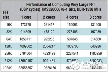
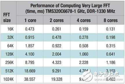
Table 1: Results of FFT and milliseconds for FFT on 1/2/4/8 DSP core respectively
What is a miniature slip ring? Miniature slip rings are rotary electrical connectors that allow power and data to be transferred between a stationary and rotating structure. They are often used in medical, military, and aerospace applications where size and weight are critical factors.
A miniature slip ring typically consists of two parts: a stationary housing and a rotating contact assembly. The contact assembly contains the brushes that make electrical contact with the rotating structure, as well as the rings that conduct current or data.
The housing can be made from any number of materials, including metals, plastics, and composites. It is typically designed to be as small and lightweight as possible while still providing adequate strength and durability.
The contact assembly is made from precious metals such as gold or silver in order to provide good electrical conductivity.
Technology improves with the continuous development of precision machinery. The more sophisticated the equipment, the smaller the volume will be. And the space that can be accommodated for installing the slip ring is also very small. The key parts of some equipment are quite a district. Especially in the high-end military, aerospace and aviation fields. 360-degree rotation is required to transmit current and signals. And the installation space is greatly reduced. It is to make the equipment work more smoothly. Therefore, it is necessary to design the slip ring to be small and exquisite. Otherwise, it won't meet the needs of the installation.
At the same time, we have moved with the continuous development of science and technology. Various high-end precision instruments have been developed. It requires the slip ring to transmit the current amount of general power. Also often undertake the transmission of weak electrical signals and various weak signals. The transmission medium is wider, and the number of loops of the slip ring is increasing.

Miniature Slip Ring,Slip Ring Parts,Slip Ring Type Induction Motor,Slip Ring Rotor
Dongguan Oubaibo Technology Co., Ltd. , https://www.sliprobs.com