For many years, it has been predicted that low dropout linear regulators (LDOs) will be withdrawn from applications in the automotive field. However, LDO regulators continue to thrive and even thrive because they are cheap and easy to use. In this article, I will explain the complexity of LDO regulators, examine the latest developments in the market (and some progress), and analyze the trend toward switching regulators as vehicle power demand continues to climb.
This article refers to the address: http://
New linear regulator
What new technology does the linear regulator have? Let us first look at the output capacitor. At present, ceramic capacitors are all selected for the 0402 package, mostly because the improved materials have increased their temperature range from 125°C (257°F) to 150°C (302°F), resulting in improved mounting methods. Thermal shock and improved vibration resistance. The small size of these capacitors reduces their inductive components, further improving high frequency performance. However, a key feature of ceramic capacitors is their low equivalent series impedance or ESR.
The basic closed-loop linear regulator system consists of an error amplifier, output driver, and load. Figures 1 through 3 detail the closed-loop frequency response of a bipolar linear regulator. The effect of changing the ESR of the output capacitor can be seen while maintaining the same system settings and output capacitance values. Capacitors with 1 ohm ESR (Figure 1) are stable; capacitors with 0.01 ohms very low ESR (Figure 2) are unstable; capacitors with 3 ohms larger ESR (Figure 3) are also unstable.
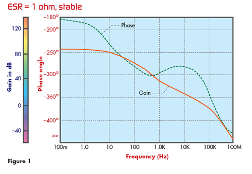
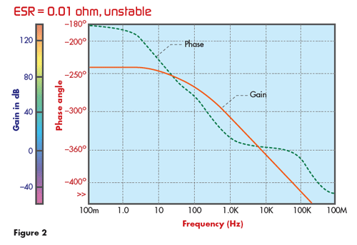
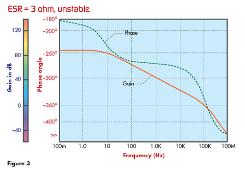
There is a very practical rule of thumb in switching power supply design: whenever the closed-loop gain is greater than or equal to 1, the closed-loop phase will never fall within 30 degrees of 360 degrees.
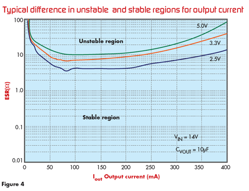
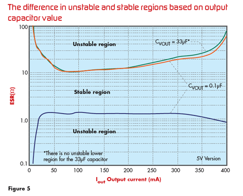
Most linear regulators do not give you access points to measure stability curves. Instead, chip fabrication provides a set of curves that correspond to the ESR values ​​of the output capacitors, showing where stability issues are likely to occur. Figure 4 shows a typical difference between the unstable and stable regions of the output capacitor ESR, which is dependent on the change in the output regulator voltage due to changes in output current. Figure 5 shows the difference between the unstable and stable regions of the output capacitor values.
The load response time typically varies inversely with the IC stability product area. Loop response time has been reduced to provide better stability. An external output capacitor can be used to compensate for most transient demands. Be sure to provide a capacitor of sufficient value for your needs. To use the commonly used capacitance equation:
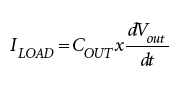
Calculate the capacitance value, transient time, and the allowable output voltage drop of the system based on the magnitude of the system load.
Quiescent current is an important indicator whether the regulator is in the load or standby state. Historically, quiescent current has not been taken seriously. With the increase in automotive electronic systems, the use of existing batteries and alternators has reached its limits. The semiconductor manufacturing process has an impact on the magnitude of the quiescent current. For products produced in two different types of manufacturing processes, we can see the impact of typical performance characteristics. Figure 6 shows the device produced in a bipolar process, while Figure 7 shows the device produced in the BCD process. Note the flat line characteristics of devices fabricated in the BCD process.
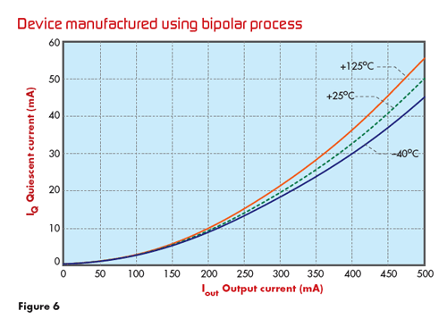
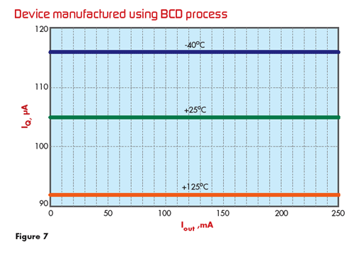
Devices using the bipolar process will increase quiescent current at high loads; devices using the BCD process will maintain low quiescent current at low loads and large loads. The result is a low contribution to the quiescent current limit of the module.
Save current
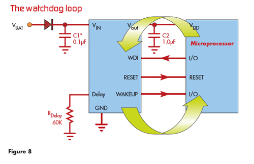
In current-saving control, you can use a watchdog regulator. The watchdog adjuster uses a wake-up signal to the microprocessor to save current. When the microprocessor instruction is starting to operate, a coordinated signal is sent back to the voltage regulator by the microprocessor, prompting the regulator that it must remain adjusted. Once the microprocessor completes the commands and instructions, the feedback signal sent back to the regulator is cancelled. The watchdog adjuster recognizes this event and sends a reset signal back to the microprocessor to turn it off, as shown in Figure 8. The end result is current savings until the microprocessor needs to issue a coordinated signal again.
Another way to save the regulator IC current is to instantly turn off the circuit that does not require operation. As long as the regulator circuit is not used immediately, it can be turned off and operated in the pulse on/off mode. This solution is best for light load conditions in cold or indoor temperatures. The higher the temperature of the device, the larger the leakage current and the more complicated the operation; the rise of the ambient temperature or the rise of the die temperature caused by the on-chip power supply will cause the operating temperature of the device to rise.
To this end, more and more people choose dual regulators (two independent output regulators on a single chip). There are several microprocessors that now require dual supply voltages. One power supply (usually a lower voltage) powers the core and the second power supply powers the I/O. By lowering the core voltage, more transistors can be integrated into the chip without letting the device temperature exceed its package limits.
Although the use of a bilinear regulator (which is more convenient, space efficient, and cost effective) does not save quiescent current, it contributes to power savings and power distribution in the system. Current savings are due to the use of shared circuits such as bandgap reference voltage and current source bias lines in the dual regulator.
Integrating multiple regulator ICs on a single chip is easy to use, saves space and cost, but is limited by the amount of power allowed in the IC.
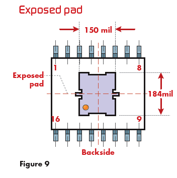
Improving the package allows a single package to consume more power. Thermal resistance can be reduced by using metal leadframe materials (exposed pads, epad). Metal-connected pins are more susceptible to heat dissipation than plastic packages. Figure 9 shows a typical exposed pad package. The device is available in a 300-mil, 16-pin SOW exposed pad package with an epad area of ​​150 mil x 184 mils.
In use, which exceeds the manufacturer's limit on device temperature (node ​​temperature is typically around 150°C / 302°F), it is possible to either damage the regulator immediately or due to differences in thermal expansion coefficients of silicon, bonding wires and plastic packages. Causes the device to fail prematurely. As the temperature rises, the failure rate increases exponentially. Research is being conducted to improve the acceptable operating temperature of these electronic components.
Switch adjuster
In addition to all the new linear regulators I have described and used, the use of switching regulators is also increasing. Switching regulators are more expensive than linear regulators because there are more external components. Diagnosing them is also a hidden cost. In essence, the characteristics exhibited by the switching regulator must be used by engineers with the ability to deal with electromagnetic interference problems.
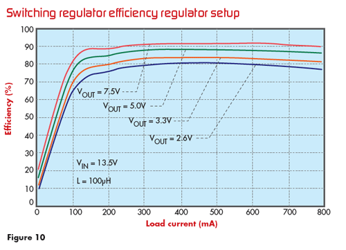
There is no doubt that switching regulators are more efficient than LDOs. As shown in Table 1, the efficiency of the switching regulator is 90%, while the efficiency of the LDO is 36%. Figure 10 shows a typical efficiency curve for a bulkhead switch regulator.
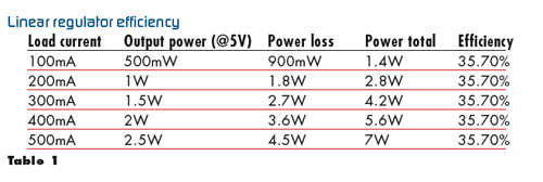
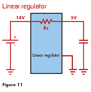
The power consumption of the linear regulator can be simply calculated as (ignoring the quiescent current) the load current multiplied by the voltage difference between the input and output. The example in Figure 11 shows that the regulator has a voltage difference of 9V, so the calculated efficiency is 35.7%, which is independent of the load, but is related to the input voltage, as described in the following example.
The only way to increase the efficiency of the linear regulator is to reduce its voltage difference. You can use the previous switching regulator (Figure 12) next to the linear regulator so that the input to the linear regulator is 6V DC, and the input in the example above is 14V DC. The switching device effectively lowers the input voltage to a more manageable voltage and distributes the voltage to drive other linear regulators. This arrangement takes advantage of the high efficiency of the switching regulator and the low cost of the linear regulator. Since the linear regulator does not have to be connected to the battery, further cost savings are achieved because lower voltage devices can be used.
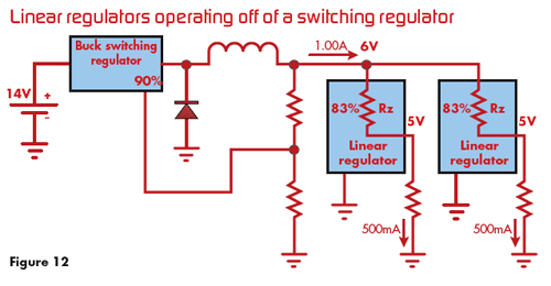
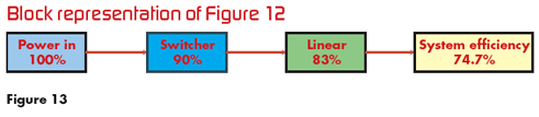
As shown in Fig. 13, the efficiency of the entire system was improved to 74.7% as compared with the efficiency of 35.7% in Fig. 11.
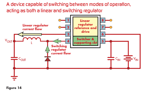
Another way to reduce current consumption is to combine the functions of the switching regulator and the linear regulator. Switching regulators are most efficient at driving loads within their design range. When the load of the output voltage is not heavy, the current required to keep the switch regulator switch working is not so much a burden as a property. Under such conditions, the linear regulator is more efficient.
The device shown in Figure 14 is capable of switching between a linear regulator and a switching regulator. The module is divided into two separate working sections: the first part (green) support system acts as a boost switch regulator; the second part (yellow) support system acts as a linear regulator. The temperature reference source that is not affected by temperature is shared by two parts. Engineers can choose to change operating modes based on maximum output load efficiency or EMI requirements. The linear regulator is more efficient when the load is very light; the switching regulator is more efficient when the load is heavy. The linear regulator's EMI performance is always better than the switching regulator.
Other applications for switching regulators include starting a car. A car with a modern anti-theft system, when trying to start a car, has to verify that the key belongs to the car. Heavy loads from the engine can cause a sharp drop in battery voltage, but they can't cause the lights to dim or the microprocessor involved in the verification process to reset.
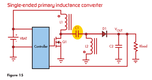
In order to do this, you need a device that can provide boost and buck for your system. One way is to use the SEPIC (single-ended primary coil inductor converter) shown in Figure 15. Capacitor C1 must be able to withstand the normal high voltage operating limits of the system (in terms of retrace pulses), and the high voltage load can clip (including other transient pulses) pulses through inductor L1. This means that a high voltage capacitor is needed to maintain maximum efficiency, and the ESR of the capacitor is low because a large current is going through the device. Some engineers hate the large current flowing through the capacitor. Overheating can cause reliability problems or aging of capacitors (open or short).
Another solution to this problem is to use a pass-through zone technology with a dual-mode converter, which creates a smooth transition between the buck and boost modes of operation, while at the same time ensuring The required buck/boost operation. As shown in Figure 16.
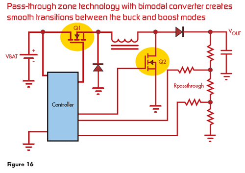
In normal operation, transistor Q1 acts as a buck switching regulator while the control circuit keeps Q2 off. When the input voltage of Vbat drops sharply, Q1 is 100% open and Q2 starts the circuit as a boost switch regulator. The resistor Rpassthrough helps set the duty transition, where there is a pass zone, and the adjusted output voltage is slightly changed to provide a smooth transition for the transition of the operating mode.
The power available in existing automotive systems is limited, and from an engineering point of view, switching regulators are much more efficient than linear regulators. Switching regulators have the most integrated functions, but they add the most to the system. Is it the most functional switching regulator now, or is it a linear regulator with fewer features? It depends on whether the consumer pays for it.
Pocket Type Nickel Cadmium Battery
The nickel–cadmium battery (NiCd battery or NiCad battery) is a type of rechargeable battery using nickel oxide hydroxide and metallic cadmium as electrodes. The abbreviation NiCd is derived from the chemical symbols of nickel (Ni) and cadmium (Cd).
Pocket Type Nickel Cadmium Battery capacity range is from 10ah to 1200ah, have three series: low discharge rate, medium discharge rate and high discharge rate.
Nickel Cadmium Batterie,Nicd Battery Pocket Plate,Railway Nicd Battery,10~1200Ah Nicd Battery
Henan Xintaihang Power Source Co.,Ltd , https://www.taihangbattery.com