ARM Cortex-M7 processor
The newest member of the Cortex-M processor family is the Cortex-M7. This new core features features that support the needs of new embedded technologies, and is designed for applications that require high processing performance, real-time responsiveness, and energy efficiency. Overall, the Cortex-M7 processor includes the following key features:
• High-performance, dual-instruction-issued 6-stage pipeline with up to two instructions per clock cycle;
• 64-bit AXI system bus interface;
• Optional instruction cache (4 to 64KB) and data cache (4 to 64KB), each with optional ECC (Error Correction Code) support;
• Optional 64-bit instruction tightly coupled memory (ITCM) and optional dual 32-bit data TCM (D{0,1}TCM), each supporting a customer ECC implementation;
• Optional low latency AHB peripheral bus interface that allows deterministic fast access to peripherals in real-time applications.
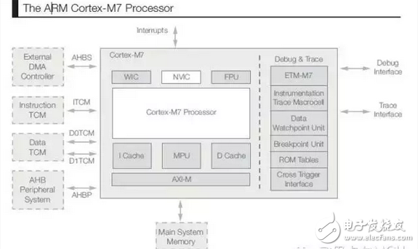
Figure 1 ARM Cortex-M7 processor
ARM Cortex-M7 processor configuration options
The microarchitecture of the Cortex-M7 processor is different from the other cores in the Cortex-M processor family. The Cortex-M7 microarchitecture features a 6-stage superscalar pipeline implementation that dramatically improves system performance by improving architectural performance (reducing the number of instruction cycles per cycle) and increasing operating frequency. To support higher instruction and data bandwidth requirements for superscalars, the key memory interface is designed to be 64-bit wide. Both the AXI system bus and the single-cycle ITCM interface are 64-bit, and the dual 32-bit D-TCM interface can handle two 32-bit transfers or one 64-bit data transfer in one cycle. Table 1 summarizes the bus in the Cortex-M7 processor microarchitecture, highlighting the comparison of the new interface to the predecessor ARM Cortex-M family of devices.
The AXI master interface provides important functions when supporting the memory expandability required for many IoT applications. Because the new usage model is based on data that is continuously collected and analyzed, it is critical to be able to leverage external memory to increase functionality. In addition to the AXI host interface, the TCM interface also provides an optimal single-cycle interface for performing the computational operations required for control. To support processor performance levels in excess of 5 CoreMarks/MHz, high-performance memory and bus interfaces are critical.
There are several factors to consider when choosing which buses to use in the SoC and how to use them, including:
• Which peripherals need to be connected to the AHB peripheral bus on the Cortex-M7 processor for low latency access?
• Which peripherals need to be accessed by the DMA controller?
• What forms of access control and memory protection are needed?
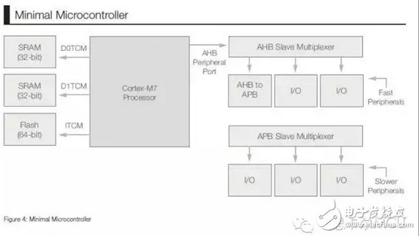
Figure 2 Minimum Microcontroller
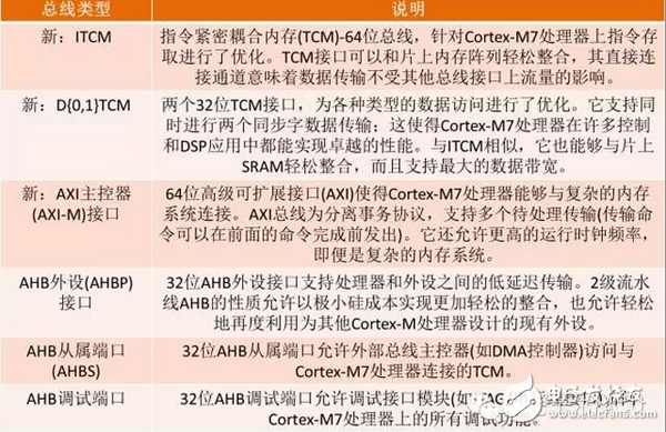
Table 1 ARM Cortex-M7 bus type and description
For example, in a very simple design, the memory system can be connected to the TCM interface, and the peripherals can be connected to the AHB peripheral interface, as shown in Figure 2. This configuration allows the SoC to not only take advantage of the scalable performance of the Cortex-M7 core, but is still able to cope with cost and size related challenges. For example, through the connection of the SRAM to the TCM interface, it is possible to support activities to implement control edge nodes that require real-time performance.
Another configuration option is to connect embedded memory and/or external memory to the AXI interface and use cache memory for higher performance. Most microcontroller applications contain many small control loops, so the number of cache misses performed by the firmware is very low. When using a cache-based design, the system may be less certain in executing programs from the AXI bus system. However, an exception vector table and an interrupt handler can be placed in the SRAM interfaced with the ITCM to implement the determined behavior when the interrupt handler is executed.
The memory scalability, performance, and efficiency benefits of AXI interfaces and caches are key to meeting application needs. This type of configuration offers many advantages over IoT applications, such as support for wireless firmware updates and data storage needs that take advantage of large external memory. However, not every application case requires every option, so the challenges associated with cost, size, and power consumption must be considered.
The memory system is designed to offer a wide range of configuration options. There are several aspects and factors to consider, including:
• Execution from an AXI or TCM interface;
• cache size (if using AXI);
• The way in which embedded memory access is accelerated, as well as the bandwidth of the flash memory;
• Optional ECC support.
Many different factors can influence decisions such as read access speed of embedded flash, clock speed requirements, and the typical size of the target application and its program popularity.
If the embedded memory access speed is similar to the required processor speed, the embedded flash can be connected to an ITCM interface with some flash access acceleration. In other cases, it would be more appropriate to use AXI with cache. If an application needs to execute a program from an external memory controller, then the memory controller will typically interface with the AXI interface, which in turn requires instruction cache and data cache support. In some cases, an application may only need to use external memory for data storage. In this case, no instruction cache is required.
Choosing the cache size largely depends on the properties of the application code. When you run your program code in embedded memory, both the instruction cache and the data cache are used, because the program image usually contains literal data, lookup tables, or read-only constants along with the instructions. Applications typically have more instruction words than data/constants inside the program image. As the size of the program grows, so does the cache requirement, and it is not uncommon for the instruction cache to be larger than the data cache. Conversely, some applications may have very small control or DSP loops, and there may be a large amount of data used as coefficients for calculations. In such cases, a larger D-cache may be more beneficial to system performance than a larger I-cache.
Of course, when optimizing performance, you also need to maximize the cache to ensure the minimum latency of larger code and data size. However, by running large cache memory at the same speed as the processor, cache lookups may consume a lot of power based on other factors. In addition, most applications' cache miss rate curves approach zero as the size increases, which means that further increases in cache size does not improve performance. Fortunately, the configurability of the Cortex-M7 core enables SoC architects to integrate a wide variety of cache sizes, from no cache to up to 64KB of instruction cache and 64KB of data cache. With this flexibility, designers can tune the SoC to meet the needs of the target application.
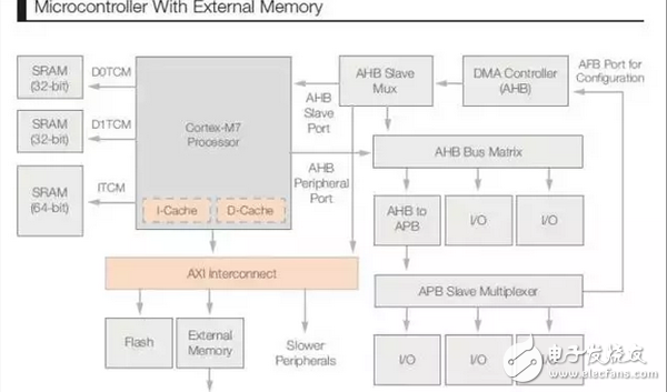
Figure 3 Microcontroller with external memory
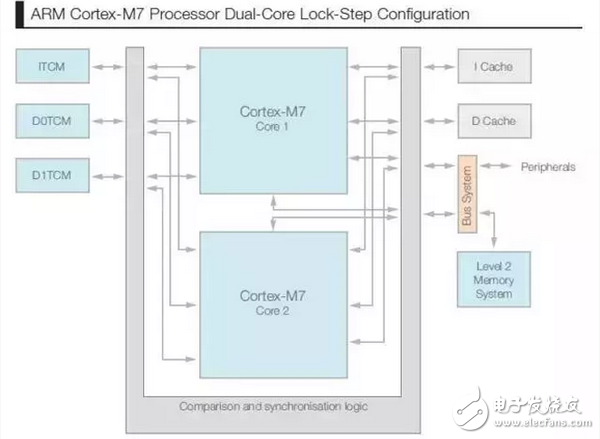
Figure 4 ARM Cortex-M7 processor dual-core lockstep configuration
In addition to the architectural options, many other features on the Cortex-M7 processor can be configured. For example, the SoC's Floating Point Unit (FPU) function can be configured to be completely free of FPU, FPU with IEEE-754 single-precision floating-point operations, or FPU that supports both IEEE-754 single-precision and double-precision operations.
Other configuration features include:
• number of interrupts, and the number of priority levels in the NVIC;
• Memory Protection Unit (MPU) configuration;
• Debug and track function;
• Functional safety related functions (ECC, dual-core lockstep).
Floating point hardware acceleration has many advantages. Obviously, the performance of floating point operations with hardware floating point units can be accelerated. In addition, memory space is optimized because hardware support reduces the number of software libraries and associated sizes required to perform floating-point operations. Reducing processing time and reducing memory footprint ultimately increases the energy efficiency of your application, clearing the barriers to performing functions that traditionally require more complex embedded systems. This advantage is very important for energy efficiency, because the floating point operation of the DSP filter can be up to 20 times faster. The single- and double-precision floating-point options also increase the scalability of the new processor.
As IoT's presentations gradually lead to technology expansion, the need to address the security and integrity challenges of embedded applications is growing. In addition to the same error exception handling and memory protection units as other Cortex-M processors, the Cortex-M7 processor also includes optional TCM memory and Cache Error Correction Code (ECC) support. This allows automatic correction of single-bit errors in memory and detection of double-bit errors.
In addition, the Cortex-M7 processor also supports dual-core lockstep configuration options. In this configuration, the core logic is instantiated twice, and the cache and TCM memory arrays are shared. This is because they can be protected by ECC and their silicon area cost can be significantly reduced (see Figure 4), resulting in a very robust fault-tolerant system design.
Implementation of Freescale KineTIs KV5x MCU Series
An example implementation of the Cortex-M7 processor is Freescale's latest release of the KineTIs KV5x MCU family, a scalable MCU family targeted for motor control and digital power conversion applications. In this SoC, some of the configuration options selected by the Cortex-M7 processor include the integration of a 16KB instruction cache and an 8KB data cache. This SoC uses the 64-bit AXI bus as an access port for embedded flash memory. Instruction cache and data cache ensure that control software residing in embedded memory is accelerated to support the level of performance required for connected industrial-level control cases. In addition to the cache, the KineTIs KV5x MCU family also integrates 64KB of SRAM connected to the ITCM interface and 128KB of SRAM interfaced to the DTCM. This provides the necessary processor local storage to support real-time control operations with minimal latency memory.
Figure 5 KineTIs KV5x MCU Series Block Diagram
The Kinetis KV5x MCU configuration is just an example of how to build an SoC to address a specific application that focuses on networked control. As time goes by, and as the number and variety of interconnect applications increases, so will the adjustments to the SoC design in the future for a wider range of configurations on the Cortex-M7 processor. The performance level will be more than doubled compared to the comparable Cortex-M4 solution, which will enable more innovation in the embedded world. With its expandability, performance and scalable capabilities, the scalable Cortex-M7 core will play an important role in supporting the "Tomorrow's Internet of Things" stage.
3 In 1 Usb Hub,Usb C Hub Vga,Type C Hub 3 In 1,Usb Hub With Vga
Shenzhen Konchang Electronic Technology Co.,Ltd , https://www.eclinusb.com