No worries, high gain: Building a low noise instrumentation amplifier with nanovolts sensitivity
Introduction
Building a voltage measurement system with nanovolt-level sensitivity encounters many design challenges. The best current op amps (such as the ultra low noise AD797) can achieve noise performance (1 kHz) below 1 nV/√Hz, but the nature of low frequency noise limits the achievable noise performance to approximately 50 nV pp (0.1). In the Hz to 10 Hz band). Oversampling and averaging can reduce the rms contribution of flatband noise, but at the expense of higher data rates and higher power consumption, but oversampling does not reduce the noise spectral density, while it is noisy in the 1/f region. no effect. In addition, to avoid noise contribution from subsequent stages, a larger front-end gain is required, which reduces system bandwidth. If there is no isolation, then all ground bounce or interference will appear at the output and potentially corrupt the low internal noise of the amplifier and its input signal. A well-behaved, low-noise instrumentation amplifier simplifies design and structure of such systems and reduces residual errors due to common-mode voltages, power supply fluctuations, and temperature drift.
The low noise instrumentation amplifier, the AD8428, delivers 2000 accurate gains with all the features necessary to solve these problems. The AD8428 features 5 ppm/°C maximum gain drift, 0.3 μV/°C maximum offset voltage drift, 140 dB minimum CMRR to 60 Hz (120 dB minimum to 50 kHz), 130 dB minimum PSRR, and 3.5 MHz bandwidth for low power Flat measurement system.
Most notable is the device's 1.3 nV/√Hz voltage noise (1 kHz) and industry-best 40 nV pp noise (0.1 Hz to 10 Hz) performance with high signal-to-noise ratio at very small signals. Two additional pins allow the designer to change the gain or add a filter to reduce the noise bandwidth. These filter pins also offer a unique way to reduce noise.
Reduce system noise with multiple AD8428 instrumentation amplifiers
The circuit configuration shown in Figure 1 can further reduce system noise. The input and filter pins of the four AD8428s are shorted to each other, reducing noise to one-half the original.
The output of any of the instrumentation amplifiers can be used to maintain a low output impedance. This circuit can be extended to reduce noise by a factor of the square root of the number of amplifiers used.
How does the circuit reduce noise?
Each AD8428 produces a typical spectral noise of 1.3 nV/√Hz converted to input (RTI), which is uncorrelated with the noise produced by other amplifiers. Uncorrelated noise sources are superimposed on the filter pins in a square and root (RSS) manner. On the other hand, the input signal is positively correlated. Each AD8428 responds to a signal that generates the same voltage on the filter pins, so connecting multiple AD8428s does not change the voltage and the gain remains at 2000.
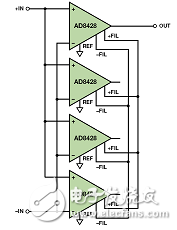
Figure 1. Noise Reduction Circuit Using Four AD8428 Instrumentation Amplifiers
Noise analysis
Analysis of the simplified version of the circuit of Figure 2 shows that connecting the two AD8428s in this way can reduce noise by a factor of √2. The noise of each AD8428 can be modeled on the +IN pin. To determine the total noise, you can ground the inputs and use the overlay to combine the noise sources.
The noise source en1 is amplified by 200 differential gain and reaches the output of the preamplifier A1. For this part of the analysis, the output of preamplifier A2 is noise-free when the input is grounded. The 6 kΩ/6 kΩ resistor divider between each output of preamplifier A1 and the output of the corresponding preamplifier A2 can be replaced by the Thevenin equivalent circuit: half of the noise level at the output of the preamplifier A1 and a 3 kΩ Series resistance. This part is the mechanism to reduce noise. A complete node analysis shows that the output voltage of the response en1 is 1000 &TImes; en1. Due to the symmetry, the output voltage of the response noise voltage en2 is 1000 &TImes; en2. Both en1 and en2 are equal to en and will be superimposed as RSS, resulting in a total output noise of 1414 &TImes; en.
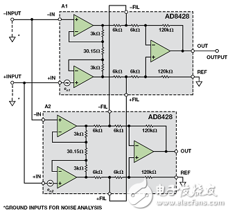
Figure 2. Noise analysis simplified circuit model
In order to fold it back to the input, the gain must be verified. Assume that a differential signal VIN is applied between +INPUT and –INPUT. The differential voltage at the first stage of the A1 output is equal to VIN × 200. The same voltage appears at the output of preamplifier A2, so no crossover signal enters the 6 kΩ/6 kΩ divider and the node analysis indicates that the output is VIN × 2000. Therefore, the total voltage noise RTI is en × 1414/2000, which is equivalent to en/√2. Using the 1.3 nV/√Hz typical noise density of the AD8428, the noise density produced by the two amplifier configurations is approximately 0.92 nV/√Hz.
After using an additional amplifier, the impedance at the filter pin changes to further reduce noise. For example, if four AD8428s are used as shown in Figure 1, the 6 kΩ resistor between the preamplifier output and the filter pins is followed by three 6 kΩ resistors, each connected to the output of each noiseless preamplifier. This effectively creates a 6 kΩ/2 kΩ resistor divider that divides the noise by four. Therefore, as predicted, the total noise of the four amplifiers is equal to en/2.
Make trade-offs between noise and power consumption
The main trade-offs come from power consumption and noise. The AD8428 has extremely high noise-to-power efficiency with an input noise density of 1.3 nV/√Hz (6.8 mA maximum supply current). For comparison, consider the low noise AD797 op amp – which requires a maximum supply current of 10.5 mA to achieve 0.9 nV/√Hz. A discrete G = 2000 low-noise instrumentation amplifier is built with two AD797 op amps and a low-power differential amplifier that can operate with two op amps and a 3.15 Ω resistor with a current of 21 mA or more. Hz noise RTI performance.
In addition to the power considerations used by many amplifiers in parallel, designers must also consider the thermal environment. A single AD8428 with a ±5 V supply will increase the temperature by approximately 8 °C due to internal power dissipation. If many devices are placed close together or placed in an enclosed space, they will conduct heat to each other, considering the use of thermal management techniques.
SPICE simulation
Although SPICE circuit simulation is not a substitute for prototyping, it is useful as a first step in validating such a circuit concept. To verify this circuit, the ADIsimPE emulator and the AD8428 SPICE macro model can be used to simulate the circuit performance when two devices are connected in parallel. The simulation results in Figure 3 show that the performance of the circuit is as expected: the gain is 2000 and the noise is reduced by 30%.
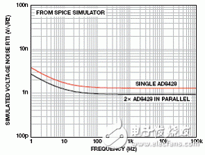
Figure 3. SPICE simulation results 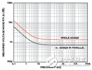
Figure 4. Voltage noise spectrum measurements for the circuit in Figure 1.
Measurement result
A complete circuit consisting of four AD8428s is measured on the bench. The measured RTI noise spectral density is 0.7 nV/√Hz (1 kHz) with 25 nV pp in the 0.1 Hz to 10 Hz range. This is less than the noise of many nanovolt meters. The measured noise spectrum and peak-to-peak noise are shown in Figures 4 and 5, respectively.
in conclusion
The nanovolt sensitivity target is very difficult to achieve and encounters many design challenges. For systems that require low noise and high gain, the AD8428 instrumentation amplifier has the features needed to achieve high performance design. In addition, the device's unique configuration allows this unusual circuit to be added to its nanovolt toolbox.
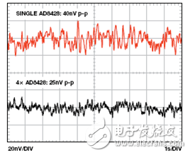
Figure 5. 0.1 Hz to 10 Hz RTI noise measured by the circuit in Figure 1.
references
MT-047 Guide: Op amp noise.
MT-048 Guide: Op amp noise relationships: 1/f noise, root mean square (RMS) noise, and equivalent noise bandwidth.
MT-049 Guide: Calculation of the total output noise of an op amp in a single-pole system.
MT-050 Guide: Calculation of the total output noise of an op amp in a second-order system.
MT-065 Guide: Instrumentation Amplifier Noise.
LED street lamp refers to the street lamp made with LED light source, which has the unique advantages of high efficiency, safety, energy saving, environmental protection, long life, fast response speed, high color rendering index, and is of great significance to urban lighting energy saving.
Led Road Light,Led Off Road Lights,Led Roadway Lighting,Cob Led Road Light
Yangzhou Heli Photoelectric Co., Ltd. , https://www.heli-eee.com