Summary:
This article refers to the address: http://
Based on the existing 2T2R structure of phase change memory (PCM), a ratio-oriented state definition method is proposed to realize multi-value storage of PCM under 2T2R structure. It has 8-state storage in the cell with the ability of the phase-change resistor to be programmed in four states, while verifying small size, while optimizing the PCM memory circuit will make the PCM more competitive. Also based on this ratio-oriented state definition, a new error correction code approach combining hardware and software makes it possible to misdetect all data bits.
introduction
Phase change memory (PCM) is a new type of non-volatile semiconductor memory that stores a fast phase change based on a sulfur-based compound material (such as Ge2Sb2Te5, GST) under current pulses. In PCM, the phase change memory material appears in the form of a resistor in that the phase change material can be converted into each other under conditions of a specific pulse with two different structures and different resistivities. These two states are a high resistivity amorphous state and a low resistivity polycrystalline state. Using the difference in resistance to distinguish between the two logic states "0" and "1" is the core of conventional PCM. Compared with other non-volatile storage technologies, PCM has many advantages, such as good compatibility with CMOS technology, small cell area, and high storage density. In addition, the phase change material can be programmed to have a variety of states between the fully polycrystalline and fully amorphous states, and these states do not require any excitation during static retention. This means that multi-value storage will be possible in PCM. As the feature size decreases, the phase change material in the PCM shrinks in size, and the current, time, and area required for the phase change decrease synchronously, which makes the PCM become more competitive when moving toward a small size. .
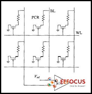
Figure 1 1T1R array
Although the size reduction can reduce the operating current, the process fluctuations are more negligible, which will cause a certain deviation in the geometry of the phase change resistor. In small sizes, the geometric size and relative change in resistance caused by the deviation may be large, especially when the chip area is large and the interference is different at various positions of the chip. Eventually, the resistance range corresponding to the two logic states will be distributed more and more divergent, which will lead to the reduction of the resistance spacing between the two logic states. This means that the system's noise margin is reduced, and the selection criteria for the peripheral sense amplifier (SenseAmplifier, S/A) and reference source will continue to increase.
For the current PCM, there are mainly two types of memory cells: 1T1R (that is, 1 transistor and 1 PCR constitutes 1 memory cell, as shown in Figure 1), and 2T2R (storage cell consists of 2 transistors and 2 phases) The structure of the phase changeresistor (PCR). Among them, BL is the bit line, WL is the word line, the same below. The 1T1R unit has a small area and high storage density, but an external reference source (such as V ref in Figure 1) is required to distinguish between two logic states ("0" and "1"). In small sizes, the closer the resistance ranges of the two logic states are, the weaker the anti-interference ability becomes, and the more stringent the requirements of the 1T1R for S/A and reference sources. The 2T2R uses two 1T1R structures to form a two-bit line complementary symmetrical output, eliminating the need for a reference source. Since the external interference on the two PCRs acting in the same unit is approximately the same, the result is equivalent to applying a common mode signal at the two inputs of the S/A, and thus has little effect on the stored information. Therefore, the reliability is high, but the storage density is much lower than the 1T1R scheme.
To the best of our knowledge, there is currently no structure that can take advantage of both. To this end, a new scheme is proposed to pursue high-density storage with better anti-jamming capability. The new scheme is based on a new method—the ratio-oriented state definition method, which uses the 2T2R structure to achieve a significant increase in storage density through multi-value storage in the unit while ensuring high anti-interference capability. Based on this state definition, an ECC method combining soft and hard is proposed.
The proposed and implemented new solution depends on two factors: First, PCR must have the characteristics of multi-value writing. This point was first confirmed in Ovshinsky's patent, and related literature has also been reported. Second, the phase change material should have a large dynamic range of resistance change. A lot of literature has shown that the difference in resistivity before and after phase transition is 100 to 1000 times, which is sufficient for the unique state definition method in the new scheme here or the new ECC.
Ratio-oriented state definition and PCM multi-value storage
In the new scheme based on the 2T2R structure, the ratio of the two PCR resistors in the same unit determines the state of the information stored in the unit. The large dynamic range of the phase change material itself provides a "spacious" one-dimensional ratio space (ODRS) for the resistance ratio of the two PCRs in the same unit (2T2R). This space can be divided into multiple intervals to represent a variety of different states. Targeting each 2T2R unit to store a 3-digit binary number (ie, 8-state), the resistance ratio has 8 different values ​​(or different ranges), requiring each PCR to be programmed into 4 different resistance ranges. State, ie R1, R2, R3, R4, where R1 < R2 < R3 < R4. There are 4 possible states for each PCR, corresponding to 4 resistance ranges, and there are multiple cases for the resistance ratio of 2 PCRs. Here, the following eight kinds of resistance ratios represent the 8-state as an example to realize the storage of 3-bit binary information per unit. The eight resistance ratios are: R1/R4, R2/R4, R1/R3, R1/R2, R2/R1, R3/R1, R4/R2 and R4/R1, as shown in Figure 2. The intervals of various states are divided by 7 preset boundary numbers (1, a, b, c, 1/a, 1/b, 1/c).
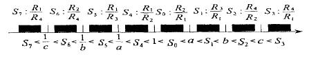
Figure 2 Definition and differentiation of 8-states in a one-dimensional ratio space
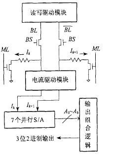
Figure 3 storage unit and peripheral read circuit
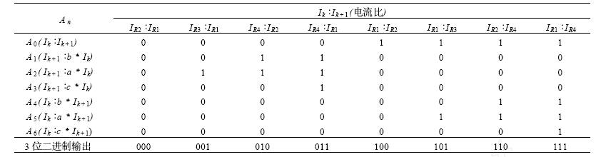
Figure 3 is a schematic diagram of the 2T2R structure and peripheral read circuit under the new scheme. The BS signal turns on the selected bit line while maintaining the same bit line voltage for the read operation. The current drive module produces currents Ik and Ik+1 equivalent to the current flowing through the PCR for S/A comparison. The peripheral read circuit includes a current drive module and seven parallel S/A and output combination logic sections. The 7 parallel S/A compares the resistance ratio of the 2 PCRs in the selected cell to the 7 boundary numbers in Figure 2. The corresponding results are shown in Table 1.
In Table 1, A n ( n = 0 to 6) represents the comparison result of each S/A, and IRx ( x = 1 to 4) is the current flowing through the phase change resistor Rx. At the same voltage, the current ratio I Rx : IRy ( x , y = 1 ~ 4 ) reflects the resistance ratio of the two resistors in the same unit. In Table 1, when IRx is less than m times IRy, the comparison result is "0", and vice versa is "1". For example, when A 0 to A 6 are “0000000â€, “000000†of A 1 to A 6 means that the current ratio Ik/Ik+1 is smaller than a and the reciprocal I k+1/Ik is also smaller than a. Only those conditions that meet this condition are: R2/R1 or R1/R2 (here, the resistance of the odd-numbered bit line is assumed to be a numerator, and the even-numbered bit line is connected to the denominator, the same below). And A 0 of "0" means that the PCR of the odd bit line is connected, and the resistance is larger than the PCR connecting the even bit lines. Therefore, only the state R2/R1 is matched, and its corresponding 3-digit binary output is "000". Other things are so similar.
Table 1 Comparison output results of various states
Related SPICE models and simulation results
At present, the phase transition physical mechanism of sulfur-based compound materials has not been fully understood. Related literature has confirmed that the resistance of PCR can be controlled by the number of crystallization pulses. A corresponding PCR empirical model is presented here.
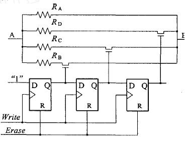
Figure 4 PCR model with 4-state
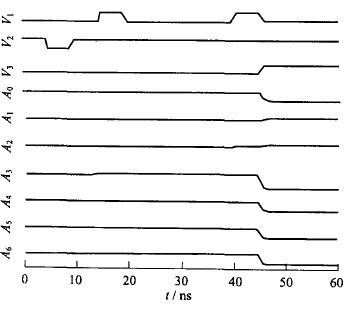
Figure 5 Write R4/R2 (A0~A 6 : "0110000")
Figure 4 shows the experimental empirical model of the proposed double-ended (A, B) 4 states (corresponding to 4 different resistance values). The PCR resistance in the figure is controlled by the number of Write pulses. The read operation has been discussed above, and the model and simulation are mainly discussed for the write operation process. Before writing, you need to first perform an Erase operation on the PCR to determine the initial state of the write. Erase is the Reset operation in PCM, which converts the PCR into a high-resistance amorphous state. The next write pulse (Set) gradually reduces the PCR resistance from the amorphous state to the polycrystalline state. In Figure 4, R is the reset end of the D flip-flop. The 4-state resistance of PCR is R1 = RA//RB//RC//RD, R2= RA//RB//RC, R3 = RA//RB, R4 = RA, (ignoring the conduction of MOS strobe Resistance RDS). The excitation source generates Set and Reset pulses when performing a write operation. The relevant circuit structure can be seen in Figure 3 of the literature. The Reset pulse is now an erase pulse, and the PCR is written as the amorphous state with the highest resistance. The Set pulse is different from the traditional 2-state storage: it is not a one-time but stepwise crystallization PCR, resulting in a variety of intermediate states between fully polymorphic and fully amorphous. The specific state transition relationship is shown in Figure 8 of the literature.
In the case of multi-valued storage, direct programming is not possible (because the programming pulse is related to the initial state). Instead, there are two ways to write it, first write it after erasing, or read it first and then write it appropriately. For read operations under multi-value storage, there are also two methods of operation, one-time parallel readout, or binary binary readout.
Figure 5 shows the simulation results for the unit written as "010". Emphasis is placed on verifying the feasibility of a new state definition. The write operation uses the "write first write" mode, and the read operation uses parallel readout to simplify control logic and timing. The memory cells and peripheral circuits are based on a 0.35 μm CMOS process and operate at 3.5 V (a portion of the peripheral circuitry operates at 5 V). The simulation uses HSPICE. Before writing, both PCRs in the selected cell are initialized (erased) to the R4 state (Figure 2, R4 represents the highest resistance amorphous state). When reading, the same excitation voltage is applied to the two PCRs in the cell, and the current on the PCR is compared to determine the resistance ratio. For the case of "010" (the final state is R4/R2), the subsequent writing is only for the PCR that connects the even bit lines. In Fig. 5, from top to bottom are timing waveform diagrams of the write pulse V 1 , the erase pulse V 2 (initialization), the S/A precharge pulse V 3 , and the output comparison results A 0 to A 6 , respectively. According to Table 1, after initialization, two consecutive pulses on the even bit line can convert the PCR connected to the bit line from R4 state to R2, and the comparison output result A 0~ A 6 should be “0110000†(corresponding to 3 Bit binary output "010"). The simulation results are in complete agreement.
Optimization
Optimization of read and write operations
Write: The read operation in PCM consumes very little power, and the read operation is much faster than the write and erase operations (especially compared to the SET operation of the crystallization PCR), so the pre-read after writing is written relative to the first erase after write mode. Both power and speed have advantages.
Read: The fast read operation and low power consumption of the PCM facilitates the use of the binary sense read mode rather than the parallel mode, and its peripheral circuitry is relatively simple in 8-state memory. Therefore, the read-ahead write mode and the binary-segment serial read mode are used.
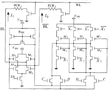
Figure 6 S/A for 7 different comparisons
Peripheral circuit optimization
In the binary sense read mode, the seven S/A and corresponding current drive modules required for parallel readout are replaced by a configurable S/A, as shown in Figure 6. The S/A can perform 7 different comparisons. Among them, the width to length ratio of M3, M5 and M7 are respectively ba, a-1 and ca times of M1. The width to length ratio of M4, M6 and M8 is b - a , a - 1 and c - a times of M2. Reasonable setting of control signals X1, X2, X3, C and D can achieve various comparisons of the two input currents I0 and I1, such as I0 and b times I1 comparison. With this S/A, the number of peripheral S/A is significantly reduced, which is beneficial to increase the storage density. At the same time, since the PCM read operation speed is faster than the write operation, the serial read has little effect on the speed of the circuit.
New soft and hard combined ECC error correction method
For the possible errors in information storage, the traditional method is to apply ECC check error correction, represented by Hamming code. However, the circuit structure required for this method is complicated, expensive, and reduces the storage density.
For PCM, the error is mainly reflected in the resistance drift of PCR. Here, based on the state definition guided by the ratio, an ECC method combining hardware and software is proposed based on the large dynamic resistance range of PCR.
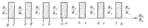
Figure 7 8-state definition with DEM function and its distribution
Figure 7 is a state distribution diagram with drift error monitoring (DEM). The large dynamic resistance variation range provided by the phase change material allows the one-dimensional interval of the ratio to have sufficient space for use after dividing the intervals corresponding to the various storage states. These remaining spaces can be divided into several parts and located between the ratio intervals corresponding to the respective storage states, which are called "forbidden zones", as indicated by the hatching. That is, once the resistance ratios of two PCRs in the same unit (RO/RE, RO, RE are the PCR resistance values ​​on the odd and even bit lines, respectively) fall into these forbidden areas, it is considered that an error has occurred. The two PCRs in the 2T2R unit are almost the same interference from the outside world, and almost the same degree of resistance drift will keep the resistance ratio basically unchanged. Therefore, the resistance resistance ratio is difficult to overcome these “forbidden zones†and jump directly from one state to another. Another state. Therefore, once an error occurs, the original correct state must be one of the two states immediately adjacent to the "forbidden zone" (instead of being judged in 8 states as in the conventional ECC). This greatly reduces the difficulty of subsequent ECC in finding and correcting errors, simplifies the peripheral circuits, and facilitates safe storage at high density.
Since the process of monitoring whether a data bit is erroneous does not depend on other data bits, this method can achieve "all-error-detection (AED)" that is difficult to implement by conventional methods. Error monitoring is achieved by two peripheral S/A and associated comparison circuits as shown in Figure 6: one S/A uses the lower limit of each “forbidden zone†(1/g, 1/e, 1/c, 1/ a , b , d , f ) are compared with the resistance ratio: the other S/A uses the corresponding upper limit (1/f , 1 / d , 1 / c , a , c , e , g ) and the resistance Compare with. When the two boundary values ​​(such as a and 1/a) of a certain "forbidden zone" are different from the resistance ratio, it means that the resistance ratio at this time has fallen into the restricted zone (a and 1/a correspond to each other). For the restricted zone [1/a , a ]), the possible original state may only be one of the 2 states immediately adjacent to the restricted zone (the restricted zone is [1/a , a ], then the possible 2 state is R2/R1 or R1/ R2). The subsequent ECC circuit continues to judge from this reduced range, and the circuit complexity will be greatly simplified (the specific circuit is omitted here). The comparison results of the normal state are shown in Table 2.

Table 2 Truth Table of Output Status with ECC Circuit
Terminals refer to Terminal Connectors,which are divided into single holes,double holes,sockets, hooks etc.From materials:copper plating, copper galvanizing, copper,aluminum,iron,etc.Their role is mainly to transmit electrical signals or to conduct electricity.
Our company's Terminal Connectors are divided into these series(as follow),which are hot-selling in recent few years:
Copper Tube Connectors(GTY)
JGK End Junction Terminal Connectors
JGA End Junction Terminal Connectors
JGY End Junction Terminal Connectors
JGB End Junction Terminal Connectors
DTL-1 Aluminium-Copper Terminal Connector
DTL-2 Aluminium-Copper Terminal Connector
DT Copper End Junction Terminals
DL Aluminium End Junction Terminals
Bus-Bar Terminal Connector
SM Insulate Terminal Connectors
One hole long barrel copper lugs
Two holes long barrel copper lugs
Terminal Connector
Terminal Connectors,Sc Cable Lug,Cable Lug,Terminal Lug
Ningbo Bond Industrial Electric Co., Ltd. , https://www.bondelectro.com