Abstract: The offset tolerance of the LVDS deserializer is used to express its jitter tolerance. This application note describes the conditions for limiting the offset tolerance and gives the steps to measure the offset tolerance of the 4-channel deserializer.
Introduction The offset tolerance of the TLVDS deserializer is used to express its jitter tolerance. Application Note 3821: Skew Margin Measurement for 4-Channel (3 Data Channels Plus Clock Channel) LVDS Serializers / Deserializers demonstrates methods for measuring offset tolerance using serializers and LVDS links. This application note describes how to measure the offset tolerance using a deserializer. The test procedure provided is applicable to any LVDS deserializer.
Receive Offset Tolerance (RSKM) RSKM refers to the effective time window in which the deserializer can correctly collect LVDS input data. In order to collect data within the data bit period (unit interval or UI), a timing strobe signal needs to be generated by the LVDS input clock. Ideally, the strobe signal is in the middle of the data pulse, so the maximum RSKM is close to half of the LVDS data bit period. However, in many non-ideal situations, internal and external conditions will reduce the timing tolerance and bring it close to the closing point of the sampling window, resulting in data "errors".
The internal parameters of the chipset that limit RSKM are listed below: The internal strobe of the deserializer is uncertain, and the position of the transmitted pulse is related to the data establishment and timing requirements, that is, the data bits output by the serializer are relative to the serializer LVDS clock. Location changes. Other factors that reduce RSKM are related to LVDS links, including: Cable Offset Intersymbol Interference (ISI) The parallel input clock jitter passed from the serializer to the deserializer improves RSKM. The main factor affecting cable offset is the cable Length, cable type and cable quality. The following suggestions help to improve the RSKM of the design: Use short, high-quality cables with low unit length deviation (10–20 ps / ft). Note that the total offset of the channel also includes the offset caused by the connector and PCB routing. High-quality connectors and good circuit board wiring (such as matching wiring length) only add a small amount of offset, and even avoid offset. Use short cables, DC balance mode, and line equalizer to minimize the impact of ISI. Providing a low-noise input clock to the serializer helps to improve the data / clock jitter specifications and maintain good offset tolerance. At the same time, good transmission line termination can avoid reflections, maintain signal integrity, and reduce skew. Recommended equipment Agilent ™ 8133A pulse generator
Tektronix® CSA8000 or similar digital oscilloscope
Tektronix P6248 differential probe
Tektronix 1103 TEKPROBE BNC â„¢ power supply
SMA cable DC power supply
The test procedure configures the deserializer in DC balance mode. Figure 1 shows the AC coupling configuration, and Figure 2 shows the timing relationship between clock and data.
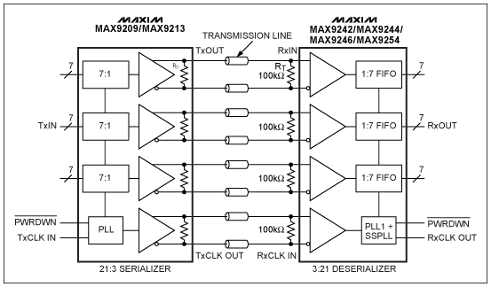
Figure 1. AC coupling configuration of the MAX9242 / 44/46/54 deserializer in DC balanced mode
Figure 2. The timing relationship between the serial input clock and data of the deserializer in DC balanced mode
Use the same length of cable to connect the differential output of the Agilent 8133A pulse generator channel 1 to the RxIN0- and RxIN0 + inputs of the 4-channel deserializer (MAX9236, MAX9244, etc.). Follow the steps below to configure correctly: Select 32MHz clock frequency, select pulse mode, use 11.1% duty cycle (1/9), select COMP button (signal compatible), use the following signal levels: high = 1.5V, low = 1.0V (DC offset = VCM = 1.25V) Connect the differential output of the Aglient 8133A pulse generator channel 2 to the RxCLKIN + to RxCLKIN- inputs of the deserializer. Using the same signal level, repeat steps 2a–2e.
Figure 3 shows the data and clock signal waveforms obtained according to the method described in steps 1–3.
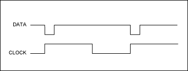
Figure 3. Data and clock signal waveforms generated in accordance with test setup steps 1–3
Use a sampling oscilloscope with a differential probe to measure the clock. Then, connect the same probe to the differential data input to make the following measurements: Figure 4 shows the clock and data header misalignment. Ideally, the clock and data intersect at a differential ground level. If this is not the case, then delay the data to align it with the clock, please use the “delay†option of Channel 8 of the Aglient 8133A pulse generator. Usually called "delay deviation".
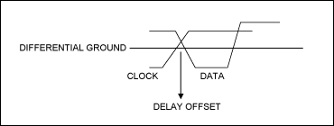
Figure 4. Clock and data misalignment / deviation
Monitor the RxOUT0 pin of the deserializer. Under normal operating conditions, this pin should be VCC. Increase the data delay, while using a multimeter to monitor the RxOUT0 level. Record the delay value when the RxOUT0 signal changes from 1 to 0. Record as: "+ delay". Next, reduce the delay to the negative region, and record the delay value when RxOUT0 changes from 1 to 0 again. Recorded as: "-delay". "+ Delay" minus the delay deviation is "RSKM-". "-Delay" plus the delay deviation is recorded as "RSKM +". Figure 5 shows the range of RSKM- and RSKM + relative to the internal strobe signal of the deserializer. Ideally, RSKM + and RSKM- should be equal; however, in reality, the two are usually different. Note that the closer RSKM + and RSKM- are to the same value, the better the offset tolerance of the device.
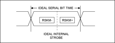
Figure 5. Relationship between RSKM +, RSKM- and strobe signals
Introduction The offset tolerance of the TLVDS deserializer is used to express its jitter tolerance. Application Note 3821: Skew Margin Measurement for 4-Channel (3 Data Channels Plus Clock Channel) LVDS Serializers / Deserializers demonstrates methods for measuring offset tolerance using serializers and LVDS links. This application note describes how to measure the offset tolerance using a deserializer. The test procedure provided is applicable to any LVDS deserializer.
Receive Offset Tolerance (RSKM) RSKM refers to the effective time window in which the deserializer can correctly collect LVDS input data. In order to collect data within the data bit period (unit interval or UI), a timing strobe signal needs to be generated by the LVDS input clock. Ideally, the strobe signal is in the middle of the data pulse, so the maximum RSKM is close to half of the LVDS data bit period. However, in many non-ideal situations, internal and external conditions will reduce the timing tolerance and bring it close to the closing point of the sampling window, resulting in data "errors".
The internal parameters of the chipset that limit RSKM are listed below: The internal strobe of the deserializer is uncertain, and the position of the transmitted pulse is related to the data establishment and timing requirements, that is, the data bits output by the serializer are relative to the serializer LVDS clock. Location changes. Other factors that reduce RSKM are related to LVDS links, including: Cable Offset Intersymbol Interference (ISI) The parallel input clock jitter passed from the serializer to the deserializer improves RSKM. The main factor affecting cable offset is the cable Length, cable type and cable quality. The following suggestions help to improve the RSKM of the design: Use short, high-quality cables with low unit length deviation (10–20 ps / ft). Note that the total offset of the channel also includes the offset caused by the connector and PCB routing. High-quality connectors and good circuit board wiring (such as matching wiring length) only add a small amount of offset, and even avoid offset. Use short cables, DC balance mode, and line equalizer to minimize the impact of ISI. Providing a low-noise input clock to the serializer helps to improve the data / clock jitter specifications and maintain good offset tolerance. At the same time, good transmission line termination can avoid reflections, maintain signal integrity, and reduce skew. Recommended equipment Agilent ™ 8133A pulse generator
Tektronix® CSA8000 or similar digital oscilloscope
Tektronix P6248 differential probe
Tektronix 1103 TEKPROBE BNC â„¢ power supply
SMA cable DC power supply
The test procedure configures the deserializer in DC balance mode. Figure 1 shows the AC coupling configuration, and Figure 2 shows the timing relationship between clock and data.
Figure 1. AC coupling configuration of the MAX9242 / 44/46/54 deserializer in DC balanced mode
Figure 2. The timing relationship between the serial input clock and data of the deserializer in DC balanced mode
Use the same length of cable to connect the differential output of the Agilent 8133A pulse generator channel 1 to the RxIN0- and RxIN0 + inputs of the 4-channel deserializer (MAX9236, MAX9244, etc.). Follow the steps below to configure correctly: Select 32MHz clock frequency, select pulse mode, use 11.1% duty cycle (1/9), select COMP button (signal compatible), use the following signal levels: high = 1.5V, low = 1.0V (DC offset = VCM = 1.25V) Connect the differential output of the Aglient 8133A pulse generator channel 2 to the RxCLKIN + to RxCLKIN- inputs of the deserializer. Using the same signal level, repeat steps 2a–2e.
Figure 3 shows the data and clock signal waveforms obtained according to the method described in steps 1–3.
Figure 3. Data and clock signal waveforms generated in accordance with test setup steps 1–3
Use a sampling oscilloscope with a differential probe to measure the clock. Then, connect the same probe to the differential data input to make the following measurements: Figure 4 shows the clock and data header misalignment. Ideally, the clock and data intersect at a differential ground level. If this is not the case, then delay the data to align it with the clock, please use the “delay†option of Channel 8 of the Aglient 8133A pulse generator. Usually called "delay deviation".
Figure 4. Clock and data misalignment / deviation
Monitor the RxOUT0 pin of the deserializer. Under normal operating conditions, this pin should be VCC. Increase the data delay, while using a multimeter to monitor the RxOUT0 level. Record the delay value when the RxOUT0 signal changes from 1 to 0. Record as: "+ delay". Next, reduce the delay to the negative region, and record the delay value when RxOUT0 changes from 1 to 0 again. Recorded as: "-delay". "+ Delay" minus the delay deviation is "RSKM-". "-Delay" plus the delay deviation is recorded as "RSKM +". Figure 5 shows the range of RSKM- and RSKM + relative to the internal strobe signal of the deserializer. Ideally, RSKM + and RSKM- should be equal; however, in reality, the two are usually different. Note that the closer RSKM + and RSKM- are to the same value, the better the offset tolerance of the device.
Figure 5. Relationship between RSKM +, RSKM- and strobe signals
SHENZHEN CHONDEKUAI TECHNOLOGY CO.LTD , https://www.szfourinone.com