Abstract: A portable GNSS navigation signal acquisition and playback system based on ARM and FPGA is designed. The system collects navigation satellite signals in complex situations and has gain control, providing a specific source for navigation receiver testing. The system converts the navigation satellite signal into a digital intermediate frequency signal through the RF circuit, and saves it to the SATA hard disk through the FPGA processing. The ARM processor acts as a monitoring terminal to send commands to the FPGA, controls the FPGA to perform data acquisition and playback, and simultaneously receives the message sent by the monitoring receiver serial port, extracts the carrier-to-noise ratio information, and draws a carrier-to-noise ratio histogram. The ARM end of the system is based on the embedded Linux system development. It uses Qt4 to design the user graphical interface, which is scalable and portable, which provides guarantee for the subsequent development of the system. The experimental results show that the signal quality of the system meets the requirements, and the data processing time of the ARM monitoring terminal is between 200 ms and 500 ms, and the real-time performance is good.
0 Preface
At present, the application of GNSS satellite navigation and positioning system is more and more extensive, including China, the United States, the European Union, Russia and other major world powers are actively deploying their own global satellite navigation and positioning system [1]. Although China started late in satellite navigation, its technology has developed rapidly. With the gradual improvement of China's Beidou 2 satellite navigation system, China has become the third country with a complete navigation system after the United States and Russia. There is an increasing demand for navigation receivers in the domestic market. Designing high-performance, multi-mode, low-cost navigation receivers has become a research hotspot. As an indispensable equipment in the development of navigation receivers, the acquisition and playback system has broad application prospects. Therefore, it is urgent to design a GNSS navigation signal acquisition and playback system with low price, good portability, intuitive interface and strong operability.
In summary, the monitoring terminal of the system uses an ARM processor based on the CortexA8 series. The processor also takes into account the cost and performance requirements, and can design a beautiful graphical operation interface. The system works at two frequency points of BD2-B1 and GPS-L1. It has good portability and intuitive interface. It can be operated by two buttons or touch screen. At the same time, it can collect navigation satellite signals in outdoor complex environment at any time, greatly improving the system. Navigation receiver development efficiency and quality.
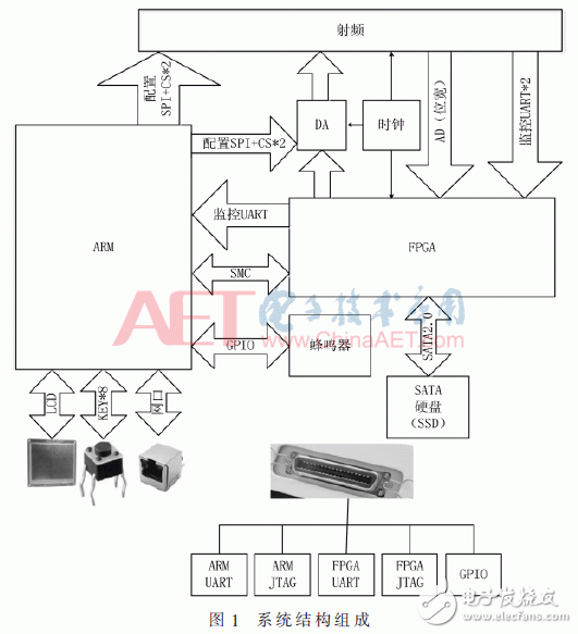
1 system structureThe system is divided into two parts: RF module and baseband module. The radio frequency module is responsible for receiving and transmitting the radio frequency signal, and converting the radio frequency signal into a baseband signal and then processing it by the baseband module; the baseband module performs functions such as user interaction and interface docking. It also includes SSD hard drives (data storage media for storing captured and playback data) as well as external interfaces. The structural composition of the system is shown in Figure 1.
2.1 RF module
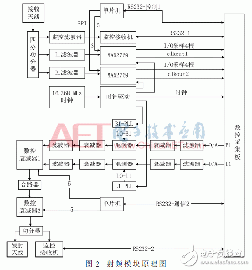
The RF module can be divided into two parts: up-conversion and down-conversion. The core device of the down-conversion part uses the MAX2769B chip, which is a multi-mode navigation receiver chip for GPS/Beidou/GLONASS/Galileo satellite navigation. GPS. The gain control device of the upconversion part adopts HMC472LP4 digital control attenuation chip. The attenuation chip is stepped by 0.5 dB and the maximum attenuation is 31.5 dB. It is controlled by 6 pins of V1~V6, and is active low. The up-and-down conversion parts are all configured with C8051F230 MCU. The down-conversion part uses GPIO port analog SPI interface to write configuration words to MAX2769B chip and configure related parameters. The up-conversion module controls the gain by controlling the level of 12 GPIO ports. At the same time, the up-and-down conversion part of the RF module adopts the ATGM332D navigation receiver of Hangzhou Zhongke Microelectronics as the monitoring receiver. The upper and lower frequency conversion modules respectively send the message information received by the monitoring receiver to the FPGA module through the serial port, and the FPGA selects the output to ARM side. Figure 2 shows the schematic diagram of the RF module [2].
2.2 baseband module
The baseband module can be divided into three parts: FPGA module, ARM module and baseband backplane. The baseband backplane is a bridge connecting the modules, and all functions except ARM and FPGA are completed. Each module is connected to the backplane in the form of a connector. Here, the SSD hard disk is innovatively used for data storage, which satisfies the demand for large-capacity space for collecting data for a long time. Due to the high complexity of the system, this paper only introduces the design scheme of the power supply and clock circuit for the baseband sub-module.
2.2.1 FPGA Module
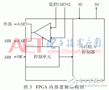
The FPGA uses Xilinx's XC7K325TFFG900-2 type FPGA (hereinafter referred to as K7). The K7 series is Xilinx's latest low-cost, high-performance FPGA for the low-end market [3]. K7 core board is mainly responsible for docking RF data interface and high-speed transceiver interface. The internal logic structure of FPGA is shown in Figure 3. According to the function, it is roughly divided into three parts: control unit, SATA controller and UART branch unit. The control unit of the FPGA is mainly responsible for the error control of the system and the communication with the ARM. Here ARM and FPGA are communicated through the SMC bus, and the SMC bus driver of the K7 processor needs to be written in the Linux kernel [4].
2.2.2 ARM module
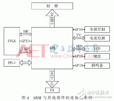
The ARM module uses the Atmel SAMA5D31 processor, which is based on the Cortex-A5 architecture and runs at 528 MHz. It integrates a floating-point unit and is a high-performance, low-power embedded processor. The ARM module integrates 256 MB ROM and 256 MB RAM to ensure performance while reducing development costs. For this system, the selection of this module is based on the results of performance, power consumption, price and other comprehensive factors [5]. ARM as the main control chip controls the entire system flow, Figure 4 shows the connection diagram between ARM and other components.
2.2.3 baseband backplane (power and clock)
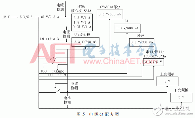
This design uses a 5 V to 42 V wide-voltage power supply input. According to the current required for each device, a 12 V/5 A adapter is used as the input power. The overall power distribution is shown in Figure 5.
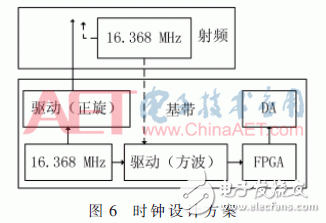
There are two clock sources for the whole system, all of which are 16.368 MHz active crystal oscillators, which are located in the baseband backplane (main clock) and RF board (backup clock). The master clock is used under normal conditions and the alternate clock is used in special applications. In addition to the 16.368 MHz clock, the ARM has its own passive crystal oscillator as its own clock source. The module communicates asynchronously to avoid errors caused by clock errors. Figure 6 shows the clock design of the system.
3.1 FPGA programming
When the system collects data, the FPGA receives the 8-bit AD digital signal (L1+B1) from the down-conversion module, and after processing, it is stored in the SSD hard disk through the SATA interface to complete data collection and storage [6]; during playback The FPGA reads data from the SSD hard disk, and after DA digital-to-analog conversion, it is sent to the up-conversion module to complete the signal broadcast [7]. During satellite signal acquisition and playback, the FPGA receives the UART information from the up- and down-conversion module monitoring receiver to determine whether the collected and broadcasted signals are normal.
This design uses the VHDL language [8] to describe the circuit that needs to be implemented. The number of high-speed transceivers (GTX) integrated in Xilinx's K7 series FPGA is up to 16 and the rate of a single GTX can reach 12.5 Gb/s. GTX is SATA. The core device of the protocol is more than enough to implement the SATA2.0 controller. This paper uses K7 to implement the physical layer, link layer and transport layer of SATA protocol, including completion of link initialization, frame encapsulation, frame transmission/pause/end control, frame parsing and verification. The transport layer of the SATA protocol is implemented by the Gigabit-level transceiver GTX, the OBB control module, and the interface transmission rate selection module. The main functions of GTX include 16B/20B encoding/decoding, serial/parallel conversion, comma detection, clock correction, prediction weight and linear equalization. The OBB control module is used for the power-on process of the hard disk or the hardware reset process, and establishes a communication link with the SATA controller.
3.2 ARM programming
As the core control module of the system, the ARM module is responsible for the scheduling of each task, and requires a friendly user interface. Therefore, embedded Linux is used as the operating system of the ARM module. According to ARM tasks, it can be roughly divided into: user interaction, module instruction configuration, data file management, and module status monitoring.
First of all, you need to implement the driver of the corresponding interface in the Linux kernel. In addition to the SMC bus driver, the driver of other interfaces has been provided in the kernel of linux3.6.9 provided by Atmel officially [9], which only needs to be extracted in the device tree file. The corresponding device node is OK. Atmel officially provides test procedures for SPI, I2C, and GPIO interfaces, and can directly transplant the corresponding programs to Qt4 for implementing the corresponding functions. The UART interface needs special emphasis here. There is no specific class for serial communication in Qt4. This system refers to the third-party qextserialport class and customizes a PortSetTIngs type structure for storing serial port parameters. Since the Linux system does not support the serial port interrupt mode, a new timer QTImer needs to be created here, and the timing is 1 s, and the serial port transmission and reception synchronization is realized in the program. Next, call the open() function to open the serial port, and call the bytesAvailable() function to determine whether the serial port data is zero. If there is data in the serial port buffer, call the readAll() function to read all the data in the buffer into the QByteArray type variable. 10].
To realize real-time receiver monitoring, it is necessary to parse the message data received by the serial port, extract the carrier-to-noise ratio information, and draw a histogram for real-time display of signal quality. This system proposes a new message parsing method for Qt4 user graphical interface. Firstly, it needs to convert QByteArray variable into QString type, and call replace() function to replace all the asterisk and carriage return in the message with Comma, and with a comma as a separator, call the split() function to split the message, look up the $GPGSV field by query, and save the satellite number and carrier-to-noise ratio into the array. According to the data in the array, use the third-party QCustomPlot class to draw the carrier-to-noise ratio histogram. First, call the setLabel function to set the horizontal and vertical coordinate names, and use the QCPBars provided by QCustomPlot to represent the histogram. Call the setData() function to perform each column. Assign, then call the addPlittable() function to add the histogram to the Widget. The abscissa assignment needs to call the setTIckVector() and setTIckVectorLabels() functions, and finally call replot() to redraw the histogram to ensure that the histogram is updated in real time.
4 Experiment and verificationDue to the superiority of Qt4 in interface design, you can change the interface style at any time according to your needs [11].
In order to verify whether the serial port blocking phenomenon occurs in the ARM terminal program and whether the real-time requirements are met, the processing time of each frame message is analyzed. The program is transplanted to the embedded development platform, and the intermediate frequency signal of a satellite is played back using the labsat loop. The intermediate frequency signal contains the information of the GPS and BD2 messages. After 3.5 hours of continuous testing, a set of data is obtained, and the data is analyzed by MATLAB. , the results shown in Figure 7 are obtained.
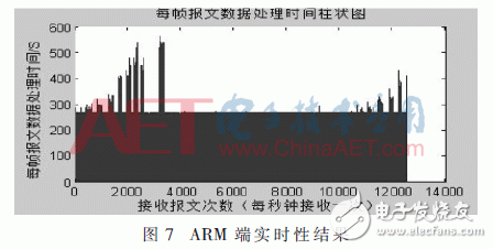
It can be clearly seen from Figure 7 that the message parsing and drawing time is about 250 ms, and occasionally the burst time will reach the peak of 550 ms, and the processing time is within 1 s, which fully meets the real-time requirements.
5 ConclusionThe portable GNSS navigation signal acquisition and playback system designed in this paper realizes the preservation and playback of satellite IF data. The monitoring terminal adopts ARM processing platform, and writes the SMC bus driver for K7 FPGA, and designs the corresponding graphical operation interface. Cost-saving while maintaining good operability of the equipment, while using SSD as a storage medium, to ensure the long-term collection requirements of the equipment. Here, using MATLAB to analyze the spectrum and power spectrum of the IF signal, the signal quality of the playback meets the requirements of the navigation receiver test, and the saved IF data provides reliable raw data for the research of the signal acquisition and tracking algorithm. It laid the foundation for the development of high performance, low price navigation receivers.
Electronic Cigarette 600 Puffs
G-Mini is a disposable unit with pre-filled salt nic e-liquid. Each mini pod vape has an estimated 400+ puffs, and built in an internal 350mAh battery which is to be disposed of once the life cycle is completed. 2ml of Salt Nic E-Liquid with the nicotine level of 30mg. 12 flavors, flat housing body, light weight, easily put it in your pocket, perfect for users on the go!
Disposable e cigarette is portable, easy to get in every e cig store, inhale-activated mechanism, no button needed, just take a drag, fast vaping!
Shenzhen Axiswell Technology Co., Ltd. Works as e-cigarettes supplier with design, research and development, manufacturing and sale team. We have experienced engineers, 8 production lines, proving OEM and ODM service. How do we control our quality? We have more than 8 QC members to carry out strict inspection: in-coming inspection (IQC), in-process inspection (IPQC) and final inspection (FQC). 100% full inspection before delivery. Our vape pens have exported to America, Europe, Asia, and are trusted by clients. We sincerely hope work with you for expanding Electronic Cigarettes market.
electronic cigarette vape pen,e-cigarette,disposable e-cigarette,e-cigarette vape,e-cigarette pod
Shenzhen Axiswell Technology Co., Ltd , https://www.medhealthycare.com