The key parts of CDMA mobile phone frequency synthesizer are analyzed, and the design scheme is proposed.
Keywords: CDMA mobile phone, radio frequency front end, frequency synthesizer, phase noise
1 Introduction With the development of mobile communication technology, CDMA is being widely used and researched as a new generation of work standards. China Unicom has initially established a CDMA network nationwide. The research and development of CDMA mobile phones has become a hot spot for major mobile phone manufacturers at home and abroad. Frequency synthesizer plays the role of heart in the radio frequency part of CDMA mobile phone. In the CDMA mobile station specification standard IS-98C, the frequency interval is required to be 30kHz, which makes the frequency synthesizer have a large frequency division ratio, which can reach more than 30,000, to meet the in-band phase in the case of a large frequency division ratio Noise requirements become a problem that needs to be solved. In addition, the design, lock time, and circuit simplicity of the higher-order loop must also be considered. This article analyzes and designs this subject, proposes solutions, and obtains good results.
2 CDMA mobile phone frequency synthesizer index requirements and analysis The CDMA mobile phone frequency synthesizer index requirements are as follows: output frequency range 954.42 ~ 979.35MHz; frequency increment 30kHz; output power range-6 ~ 0dBm; phase noise-136dBc / Hz @ 900kHz ; Conversion time 4ms.
2.1 Principle of PLL frequency synthesizer and source of noise The composition of frequency synthesizer is shown in Figure 1. Insert a variable digital divider in the feedback branch of the phase-locked loop. The loop input signal is a pulse signal with frequency fr after a high stability reference source is divided by Rref times. It and the output of the voltage-controlled oscillator are divided by N times to obtain a pulse signal with a frequency of fN, and the phase is compared in the phase detector. When the loop is locked, the output frequency fo = Nfr of the voltage-controlled oscillator, and the frequency division ratio N can be changed to change the output frequency. The output spectrum of any frequency source cannot be completely pure, and it is more or less accompanied by random phase noise and periodic spurious interference. The former is presented as a continuous spectrum, expressed by power spectral density; the latter is a concentrated line spectrum. The sources of noise are divided into two categories: one is input noise and interference; the other is internal noise and interference. These noises and interference will cause the output phase noise of the loop, making the output signal spectrum impure and the frequency stability worse.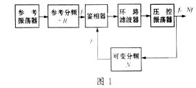
2.2 Spurious output analysis of digital single-loop phase-locked frequency synthesizer (1) The loop's ability to filter out spurious interference can be classified into three types according to the effect of the spurious interference on different positions of the loop.
The first type of interference: acts on the input of the phase detector, that is, the harmonic interference of the reference crystal. The filtering capability of the loop to the first type of interference H1
(JΩ) is:
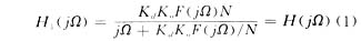
In the formula: N is the frequency division ratio of the variable frequency divider; Kd is the phase detector gain of the phase detector; Ko is the VCO voltage control sensitivity;
H (jΩ) is the loop closed-loop transfer function; F (jΩ) is the loop filter transfer function; Ω is the baseband angular frequency.
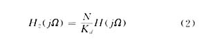
The second type of interference: acting on the output of the phase detector, mainly the ripple interference of the phase detector. The filtering capability H2 (jΩ) of the loop to the second type of interference is:
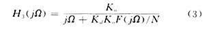
The third type of interference: acting on the input of the voltage-controlled oscillator, any interference that can enter the voltage-controlled control line belongs to this category. The filtering capability of the loop to the third type of interference is:
In summary, the loop presents low-pass filtering characteristics for the first and second types of interference, and bandpass filtering characteristics for the third type of interference. To reduce the influence of the first and second types of interference, the loop bandwidth should be as narrow as possible, but the third type of interference to Ω? Ωn should have a larger loop bandwidth. This obviously brings contradictions to the choice of loop bandwidth. The loop parameters must be selected reasonably for specific interference sources to make the loop have excellent filtering capabilities for interference.
(2) The method of reducing the output of parasitic spurious interference The parasitic spurious interference is mainly the ripple interference of the phase detector. When the loop is locked, the output voltage or current of the phase detector is actually not an ideal DC voltage or current. There are some harmful AC components. These harmful components are generally the fundamental wave and harmonics of the phase detection frequency. Ripple. If the loop fails to suppress this ripple, the ripple will tune the voltage-controlled oscillator, causing parasitic spurious interference sidebands at the output. This ripple voltage appears at the output of the phase detector and belongs to the second type of interference. According to equation (1) and modulation theory, the sideband ripple rejection ratio of the loop can be deduced as:
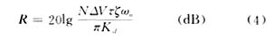
Where: N is the variable frequency divider frequency division ratio; ΔV is the amplitude of the phase detector output ripple, determined by the PLLIC used; τ is the pulse width of the phase detector output ripple, determined by the PLLIC used; Kd is the identification The phase detector gain is determined by the PLLIC used; ξ is the damping coefficient of the loop; ωn is the natural resonant angular frequency of the loop; in order to reduce the parasitic sideband caused by the ripple voltage of the VCO, in addition to design, pay attention to reduce Outside N, only decrease ωn or ξ. However, ωn cannot be too small, it is limited by the loop lock capture time. To further filter the ripple, an auxiliary filter needs to be added to the loop. The improvement of the sideband ripple rejection ratio due to the addition of a primary RC auxiliary low-pass filter is:
R ′ = 20lg (ωc / ωr) (5)
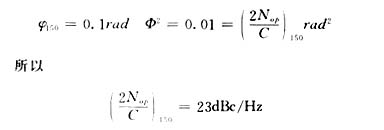
Where: ωc is the cut-off angular frequency of the RC low-pass; ωr is the phase-detection angular frequency of the loop; in order not to affect the performance of the original second-order loop, it is required: ωc≥5ωn; the value of ξ is not as small as possible, Because of the overshoot phenomenon in the transient process of the loop, the magnitude of the overshoot is related to ξ. The smaller the ξ, the greater the overshoot and the worse the relative stability of the loop. Comprehensive consideration, engineering generally choose ξ = 0.707. Imperfect power supply or jitter can also cause spurious output. The most sensitive component of the frequency synthesizer to power supply noise is the oscillator, especially a wide-tuned VCO. When the tuning slope of the VCO is 15MHz / V, it means that each μV of the root mean square ripple produces a root mean square frequency of 15Hz. At 50 Hz it indicates that the root mean square phase shift φ is 0.3 rad. The root mean square ripple component of 1μV at 150Hz gives:
From the viewpoint of both noise and ripple, no power supply should be fed directly to the tuning control part of a high slope VCO. The power supply must be connected to an operational amplifier with large power supply ripple suppression and low noise characteristics. The design of the power supply in the frequency synthesizer is very strict, especially for the VCO, in general, it must use a low noise, low ripple regulator as close to its position as possible to supply power.
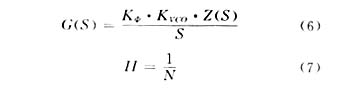
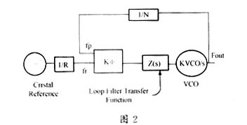
2.3 Output phase noise of digital single-loop phase-locked frequency synthesizer (1) Analysis of transfer function In single-loop digital frequency synthesizer, there are many sources of noise. Different noise sources have different contributions to the loop output noise. The phase-locked loop shown in Figure 2 defines:
The transfer functions of different phase noise sources are shown in Table 1. 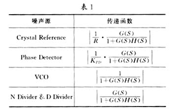
It can be seen from Table 1 that the transfer function of the phase noise of the reference source, frequency divider, and phase detector contains a common factor, namely:
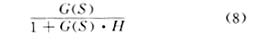
Therefore, these noise sources can be referred to as in-band noise sources. Loop bandwidth and phase margin can be defined as:
From the monotonous decreasing characteristic of G (S), the VCO can be obtained.
(2) Analysis and design of the optimal loop bandwidth From the above analysis, it can be seen that within the loop bandwidth, the phase noise of the output signal is mainly contributed by the in-band noise source. Outside the loop bandwidth, the phase noise of the output signal It is mainly caused by VCO, as shown in Figure 5. The measurement results show that when the loop bandwidth is large enough to eliminate the effect of VCO noise, the phase noise close to the carrier frequency is basically the same as the loop bandwidth

Irrelevant. When designing a phase-locked loop, in order to make the overall output phase noise performance the best, usually the intersection of the phase noise curve of the VCO in FIG. 5 and the phase noise curve of the in-band noise source (equivalent to the VCO output frequency) It is the best loop bandwidth. It should be noted that although the phase noise within the loop bandwidth mainly depends on the in-band noise source, it also contains a little noise contribution from the VCO. Especially when the loop bandwidth is very narrow and the phase noise of the VCO is very poor. 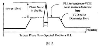
(3) Phase noise floor analysis The calculation formula of the phase noise floor is:
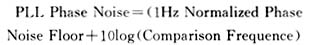
The phase noise floor is mainly determined by the process and circuit structure of the PLL manufacturer. For each octave of the phase discrimination frequency, the noise floor is improved by 3dB. Based on National Semiconductor's PLL data, the noise floor can be above -210dBc / Hz.
(4) Comprehensive consideration of output phase noise From the analysis, it can be seen that the frequency synthesizer used in CDMA mobile phones, as long as the selected reference crystal oscillator index is better (this is easy to meet and the cost is not high) The phase noise depends almost entirely on the noise floor of the phase detector, and the out-of-band phase noise depends on the phase noise performance of the uncontrolled VCO. According to the following formula, the theoretical value of in-band noise can be obtained:
3 Device selection and circuit implementation As the selection of components for frequency synthesizers used in mobile phones, usually factors such as phase noise, volume, power consumption, and price are mainly considered. The following is a brief analysis of the best indicators that can be achieved with the PLL, VCO, and TCXO we have selected.
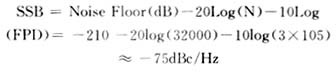
PLL uses National Semiconductor's LM2332; PLL is equivalent to 900MHz, and the effective noise floor deteriorates to -75dBc / Hz.
MURATA's VCO chip MQK002-967 can meet the requirements of the typical tuning sensitivity of 24MHz / V ± 6MHz, and its phase noise index is: -82dBC / Hz @ 1kHz, -100dBC / Hz @ 10kHz, which can be calculated by modeling · At 81 · @ 900kHz, the phase noise is better than -138dBC / Hz. The frequency stability of the TCXO frequency synthesizer depends on the stability of the TCXO. What TCXO uses is Kinseki: the frequency is 19.68MHz, the phase noise is -105dBc / Hz @ 100Hz, -125dBc / Hz @ 1kHz, -140dBc / Hz @ 10kHzOffset.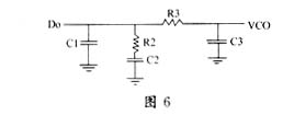
There are two types of loop filters: passive and active. Considering factors such as volume and noise, passive third-order loop filters are generally used in mobile phones. As for the determination of component parameters, many materials have given very mature empirical formulas, which will not be discussed here. The specific circuit is shown in Figure 6. Practice has proved that according to the formula:
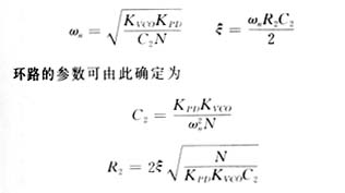
C1 can be selected as C2 / 15 <C1 <C2 / 10, and the calculation results are in good agreement with the actual.
Through debugging the connection of the circuit, it is obtained that when the loop bandwidth is 1kHz, the in-band phase noise can reach -72dBc / Hz, which is basically the same as the theoretical value. Therefore, the in-band noise is mainly generated by the phase noise floor of the phase discriminator and the frequency divider. Since the phase noise of the crystal oscillator is not large, the total frequency division ratio N / R has little effect on the in-band noise. The out-of-band noise is determined by the VCO and is -138dBc / Hz at 900kHz offset frequency, which can meet the system requirements. Due to the effect of the auxiliary filter, the ripple of the phase discrimination frequency is basically not seen. At this time, the lock time of the loop is 800 μs, which meets the circuit requirements.
references
1 Luer Rui et al. Mobile communication engineering. Beijing: People's Posts and Telecommunications Press, 1993
2 Recommended Minimum Performance Standard for Dual-Mode Wideband Spread Spectrum Cell ular MobileStaTIon. TIA / EIA ISï¼98ï¼A Interim Standard, April 1996
3 Mobile StaTIon-Base StaTIon Compatibility Standard for Dual-Mode Wideband Spread Spe ctrum CellularSystem. TIA / EIA IS-95-A, December, 1992
4 Zhang Jusheng etc. Phase lock technology. Xi'an: Xidian University Press, 1998
Keywords: CDMA mobile phone, radio frequency front end, frequency synthesizer, phase noise
1 Introduction With the development of mobile communication technology, CDMA is being widely used and researched as a new generation of work standards. China Unicom has initially established a CDMA network nationwide. The research and development of CDMA mobile phones has become a hot spot for major mobile phone manufacturers at home and abroad. Frequency synthesizer plays the role of heart in the radio frequency part of CDMA mobile phone. In the CDMA mobile station specification standard IS-98C, the frequency interval is required to be 30kHz, which makes the frequency synthesizer have a large frequency division ratio, which can reach more than 30,000, to meet the in-band phase in the case of a large frequency division ratio Noise requirements become a problem that needs to be solved. In addition, the design, lock time, and circuit simplicity of the higher-order loop must also be considered. This article analyzes and designs this subject, proposes solutions, and obtains good results.
2 CDMA mobile phone frequency synthesizer index requirements and analysis The CDMA mobile phone frequency synthesizer index requirements are as follows: output frequency range 954.42 ~ 979.35MHz; frequency increment 30kHz; output power range-6 ~ 0dBm; phase noise-136dBc / Hz @ 900kHz ; Conversion time 4ms.
2.1 Principle of PLL frequency synthesizer and source of noise The composition of frequency synthesizer is shown in Figure 1. Insert a variable digital divider in the feedback branch of the phase-locked loop. The loop input signal is a pulse signal with frequency fr after a high stability reference source is divided by Rref times. It and the output of the voltage-controlled oscillator are divided by N times to obtain a pulse signal with a frequency of fN, and the phase is compared in the phase detector. When the loop is locked, the output frequency fo = Nfr of the voltage-controlled oscillator, and the frequency division ratio N can be changed to change the output frequency. The output spectrum of any frequency source cannot be completely pure, and it is more or less accompanied by random phase noise and periodic spurious interference. The former is presented as a continuous spectrum, expressed by power spectral density; the latter is a concentrated line spectrum. The sources of noise are divided into two categories: one is input noise and interference; the other is internal noise and interference. These noises and interference will cause the output phase noise of the loop, making the output signal spectrum impure and the frequency stability worse.
The first type of interference: acts on the input of the phase detector, that is, the harmonic interference of the reference crystal. The filtering capability of the loop to the first type of interference H1
(JΩ) is:
In the formula: N is the frequency division ratio of the variable frequency divider; Kd is the phase detector gain of the phase detector; Ko is the VCO voltage control sensitivity;
H (jΩ) is the loop closed-loop transfer function; F (jΩ) is the loop filter transfer function; Ω is the baseband angular frequency.
The second type of interference: acting on the output of the phase detector, mainly the ripple interference of the phase detector. The filtering capability H2 (jΩ) of the loop to the second type of interference is:
The third type of interference: acting on the input of the voltage-controlled oscillator, any interference that can enter the voltage-controlled control line belongs to this category. The filtering capability of the loop to the third type of interference is:
In summary, the loop presents low-pass filtering characteristics for the first and second types of interference, and bandpass filtering characteristics for the third type of interference. To reduce the influence of the first and second types of interference, the loop bandwidth should be as narrow as possible, but the third type of interference to Ω? Ωn should have a larger loop bandwidth. This obviously brings contradictions to the choice of loop bandwidth. The loop parameters must be selected reasonably for specific interference sources to make the loop have excellent filtering capabilities for interference.
(2) The method of reducing the output of parasitic spurious interference The parasitic spurious interference is mainly the ripple interference of the phase detector. When the loop is locked, the output voltage or current of the phase detector is actually not an ideal DC voltage or current. There are some harmful AC components. These harmful components are generally the fundamental wave and harmonics of the phase detection frequency. Ripple. If the loop fails to suppress this ripple, the ripple will tune the voltage-controlled oscillator, causing parasitic spurious interference sidebands at the output. This ripple voltage appears at the output of the phase detector and belongs to the second type of interference. According to equation (1) and modulation theory, the sideband ripple rejection ratio of the loop can be deduced as:
Where: N is the variable frequency divider frequency division ratio; ΔV is the amplitude of the phase detector output ripple, determined by the PLLIC used; τ is the pulse width of the phase detector output ripple, determined by the PLLIC used; Kd is the identification The phase detector gain is determined by the PLLIC used; ξ is the damping coefficient of the loop; ωn is the natural resonant angular frequency of the loop; in order to reduce the parasitic sideband caused by the ripple voltage of the VCO, in addition to design, pay attention to reduce Outside N, only decrease ωn or ξ. However, ωn cannot be too small, it is limited by the loop lock capture time. To further filter the ripple, an auxiliary filter needs to be added to the loop. The improvement of the sideband ripple rejection ratio due to the addition of a primary RC auxiliary low-pass filter is:
R ′ = 20lg (ωc / ωr) (5)
Where: ωc is the cut-off angular frequency of the RC low-pass; ωr is the phase-detection angular frequency of the loop; in order not to affect the performance of the original second-order loop, it is required: ωc≥5ωn; the value of ξ is not as small as possible, Because of the overshoot phenomenon in the transient process of the loop, the magnitude of the overshoot is related to ξ. The smaller the ξ, the greater the overshoot and the worse the relative stability of the loop. Comprehensive consideration, engineering generally choose ξ = 0.707. Imperfect power supply or jitter can also cause spurious output. The most sensitive component of the frequency synthesizer to power supply noise is the oscillator, especially a wide-tuned VCO. When the tuning slope of the VCO is 15MHz / V, it means that each μV of the root mean square ripple produces a root mean square frequency of 15Hz. At 50 Hz it indicates that the root mean square phase shift φ is 0.3 rad. The root mean square ripple component of 1μV at 150Hz gives:
From the viewpoint of both noise and ripple, no power supply should be fed directly to the tuning control part of a high slope VCO. The power supply must be connected to an operational amplifier with large power supply ripple suppression and low noise characteristics. The design of the power supply in the frequency synthesizer is very strict, especially for the VCO, in general, it must use a low noise, low ripple regulator as close to its position as possible to supply power.
2.3 Output phase noise of digital single-loop phase-locked frequency synthesizer (1) Analysis of transfer function In single-loop digital frequency synthesizer, there are many sources of noise. Different noise sources have different contributions to the loop output noise. The phase-locked loop shown in Figure 2 defines:
Therefore, these noise sources can be referred to as in-band noise sources. Loop bandwidth and phase margin can be defined as:
From the monotonous decreasing characteristic of G (S), the VCO can be obtained.
(2) Analysis and design of the optimal loop bandwidth From the above analysis, it can be seen that within the loop bandwidth, the phase noise of the output signal is mainly contributed by the in-band noise source. Outside the loop bandwidth, the phase noise of the output signal It is mainly caused by VCO, as shown in Figure 5. The measurement results show that when the loop bandwidth is large enough to eliminate the effect of VCO noise, the phase noise close to the carrier frequency is basically the same as the loop bandwidth
(3) Phase noise floor analysis The calculation formula of the phase noise floor is:
The phase noise floor is mainly determined by the process and circuit structure of the PLL manufacturer. For each octave of the phase discrimination frequency, the noise floor is improved by 3dB. Based on National Semiconductor's PLL data, the noise floor can be above -210dBc / Hz.
(4) Comprehensive consideration of output phase noise From the analysis, it can be seen that the frequency synthesizer used in CDMA mobile phones, as long as the selected reference crystal oscillator index is better (this is easy to meet and the cost is not high) The phase noise depends almost entirely on the noise floor of the phase detector, and the out-of-band phase noise depends on the phase noise performance of the uncontrolled VCO. According to the following formula, the theoretical value of in-band noise can be obtained:
3 Device selection and circuit implementation As the selection of components for frequency synthesizers used in mobile phones, usually factors such as phase noise, volume, power consumption, and price are mainly considered. The following is a brief analysis of the best indicators that can be achieved with the PLL, VCO, and TCXO we have selected.
PLL uses National Semiconductor's LM2332; PLL is equivalent to 900MHz, and the effective noise floor deteriorates to -75dBc / Hz.
MURATA's VCO chip MQK002-967 can meet the requirements of the typical tuning sensitivity of 24MHz / V ± 6MHz, and its phase noise index is: -82dBC / Hz @ 1kHz, -100dBC / Hz @ 10kHz, which can be calculated by modeling · At 81 · @ 900kHz, the phase noise is better than -138dBC / Hz. The frequency stability of the TCXO frequency synthesizer depends on the stability of the TCXO. What TCXO uses is Kinseki: the frequency is 19.68MHz, the phase noise is -105dBc / Hz @ 100Hz, -125dBc / Hz @ 1kHz, -140dBc / Hz @ 10kHzOffset.
C1 can be selected as C2 / 15 <C1 <C2 / 10, and the calculation results are in good agreement with the actual.
Through debugging the connection of the circuit, it is obtained that when the loop bandwidth is 1kHz, the in-band phase noise can reach -72dBc / Hz, which is basically the same as the theoretical value. Therefore, the in-band noise is mainly generated by the phase noise floor of the phase discriminator and the frequency divider. Since the phase noise of the crystal oscillator is not large, the total frequency division ratio N / R has little effect on the in-band noise. The out-of-band noise is determined by the VCO and is -138dBc / Hz at 900kHz offset frequency, which can meet the system requirements. Due to the effect of the auxiliary filter, the ripple of the phase discrimination frequency is basically not seen. At this time, the lock time of the loop is 800 μs, which meets the circuit requirements.
references
2 Recommended Minimum Performance Standard for Dual-Mode Wideband Spread Spectrum Cell ular MobileStaTIon. TIA / EIA ISï¼98ï¼A Interim Standard, April 1996
3 Mobile StaTIon-Base StaTIon Compatibility Standard for Dual-Mode Wideband Spread Spe ctrum CellularSystem. TIA / EIA IS-95-A, December, 1992
4 Zhang Jusheng etc. Phase lock technology. Xi'an: Xidian University Press, 1998
For the Oil Immersed Aouto Transformer, we can produce voltage of 220kV, 330kV and 500kV and capacity upto 460MVA. We use the best quality of raw material and advance design software to provide low noise, low losses, low partial discharge and high short-circuit impedance for Power Transformer.
Our power transformer are widely used in national grid, city grid, rural grid, power plant, industrial and mining enterprise, and petrochemical industry.
Power Plant Transformer,Auto Power Transformer,Auto Transformer,High Quality Auto Power Transformer
Hangzhou Qiantang River Electric Group Co., Ltd.(QRE) , https://www.qretransformer.com