Plasma display power reduction technology
At the beginning of 2009, there were reports in many media at home and abroad that the EU would ban the sale of plasma TVs. Paul Gray, the head of the European Television Industry Research Association, denied this statement, but also mentioned that the association has the following plans.
â— The minimum standard of flat panel TV energy efficiency will be set, and the maximum limit of energy consumption will be set according to the different sizes of the screen
â— The standby power consumption of the TV will be compulsorily lower than 1W. This requirement will be given to manufacturers for about 1 year
It can be seen that although the EU does not really propose a proposal to ban the sale of plasma TVs, there will still be clear restrictions on the power consumption of such products, including standby power consumption and average power consumption. This forces us to make great efforts to make unremitting improvements and research on how to reduce power consumption, improve power factor, and improve luminous efficiency.
So, in what ways can optimization and improvement be started to effectively reduce the power consumption of the PDP machine? Below we conduct a qualitative analysis of this.
1 Power supply The power supply is an important part of the PDP. It requires high efficiency, small size, large transient output power, and protection functions and functions for starting different output voltages in sequence.
The traditional PDP power supply generally adopts a two-level scheme, that is, a power factor correction (PFC) level + DC / DC conversion circuit topology. They have their own switching devices and control circuits. Although it can obtain good performance, it is too large, the cost is high, and the circuit is relatively complicated. Therefore, optimizing and transforming it has become a research direction of PDP power technology.
The analysis shows that the PFC module and the scan drive electrode DC / DC conversion module both occupy a considerable proportion from the perspective of transmission energy or the volume occupied. Therefore, the transformation of these two parts has become an entry point for the optimization of PDP switching power supply.
The current optimization schemes are as follows.
â— Single-stage power factor correction circuit (SSPFC)
As shown in Figure 1, SSPFC's small size and simple circuit characteristics make it a preferred solution for the miniaturization of PDP switching power supplies. The basic principle is: the single-stage power factor correction converter circuit topology is adopted. After the full-wave rectification of the single-phase alternating current, the DC / DC conversion unit of the double-tube flyback is connected through two inductive ICS in series. In the half power frequency period, only part of the time the current of the inductor LB works continuously. When the input voltage is an AC sine wave, the input current is an approximate sine wave with high frequency ripple. The phase of the two is basically the same, thereby improving the power factor at the input.
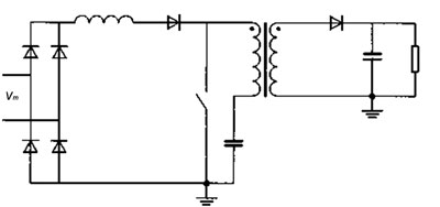
Figure 1 Single-stage power factor correction circuit
â— Using power factor control chip as shown in Figure 2, you can use MC34262 and other power factor control chips for active power factor correction.
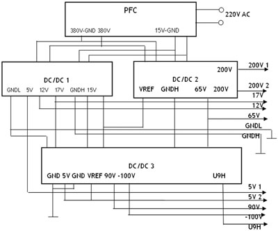
Figure 2 Power factor correction circuit using MC34262
The full-wave rectified DC voltage of the AC mains is divided and input to one input terminal of the multiplier in the control chip, and the output voltage of the error amplifier is added to the other input terminal of the multiplier. In a large dynamic range, the transmission curve of the multiplier is linear. The output voltage of the multiplier controls the threshold voltage of the current sampling comparator. When the voltage is greater than this threshold voltage, the inductor releases energy. This threshold voltage is approximately proportional to the input voltage, which is approximately proportional to the DC voltage after full-wave rectification of the AC mains. When the current in the inductor drops to zero, the inductor starts to store energy. Its average current presents a sine wave in phase with the mains voltage, which can make the power factor close to "1".
2 The drive circuit part is not only the gas discharge power consumption in the total power consumption of the PDP, because the PDP drive circuit requires a high-power, high-frequency switching circuit to provide the PDP with various high-voltage pulses required for gas discharge, although The parasitic capacitance of the PDP display screen does not consume energy, but their charging and discharging will cause energy loss in the circuit resistance and electrode lead resistance.
The voltage amplitude of the PDP drive circuit is about tens of volts negative to hundreds of volts, and the operating frequency is 100-233kHz. The design and selection of the drive circuit is particularly important for the picture quality and working efficiency of the PDP system.
In the PDP drive circuit, the address drive circuit has the highest frequency. Therefore, in addition to using the energy recovery technology in the address drive circuit, reducing the pulse voltage of the address drive circuit can also significantly reduce the address power consumption. The following methods can be used to reduce the addressing voltage pulse.
â— AwD method-namely "simultaneous display of addressing". Addressing, sustaining, and erasing pulses are applied together to reduce the addressing voltage, thereby reducing useless power consumption. At the same time, since the sustain time occupies most of the time of a subfield, the frequency of the sustain pulse can be reduced.
â— Erase addressing method-that is, enter the maintenance light-emitting stage after initialization, and after the gray level reaches the requirements, these cells are extinguished through erase addressing. Therefore, a single pixel is addressed only once per field. Moreover, lower erase voltage and current can be used to effectively reduce addressing power consumption.
â— Change the working mode of the pulse circuit-even if the switching element works as close as possible to the switching tube voltage or current close to zero (ZVS or ZCS) state, it can reduce the switching loss of the device itself.
In large-sized PDP displays, the row and column driver ICs consume a lot of energy. Its power consumption is roughly divided into three parts: logic part, level shift register and high voltage drive part. Under normal circumstances, the power consumption of the logic part is below 20mW, and the level shift register part is below 200mW. The invalid power consumption of the high-voltage drive circuit due to the charging and discharging of the screen capacitor part mainly comes from the parasitic load in the loop-the resistance component Of loss. The existence of such a resistance component is inevitable, but for the electric energy charged and discharged by the capacitor, the driver IC can manage to recover a part by means of a built-in energy recovery circuit.
In order to meet the requirements of the working performance of high-voltage devices and reduce the useless power consumption of the high-voltage driving part, the PDP driver IC needs to adopt the following stricter control measures than ordinary integrated circuits in design and process.
â— Using SOI process structure, energy loss can be greatly reduced compared with conventional power modules
â— Using dielectric isolation, the output clamping diode inside the driver IC can avoid crosstalk
â— Special treatment is given to the internal component structure and layout, etc. The internal control can eliminate the penetration current during high voltage switching
3 Selection of MOS tube Selection of appropriate power field effect transistors (MOSFETs) enables the drive circuit to work with high efficiency and stability, and the life span meets the requirements. The transition of the MOSFET is required to be fast enough to reduce the switching loss; the on-resistance is small enough to reduce the on-loss; the off-resistance is large enough to improve the isolation.
Among them, the drain-source on-resistance Rds (on), reverse recovery time trr, input capacitance Ciss and total gate charge Qg need to be carefully considered. The low on-resistance helps to reduce the conduction loss, especially the MOS tube related to the "energy recovery circuit". The low on-resistance helps to improve the efficiency of energy recovery and reduce the power consumption of the PDP. Trr, Ciss, and Qg affect the switching speed of the MOSFET. A low parameter value can speed up the conversion process of the MOSFET and help reduce the switching loss of the MOSFET. In addition, the low Ciss and Qg parameters can reduce the drive power of the MOSFET gate and simplify the design of the gate drive circuit.
The gate drive circuit is an external factor that affects the switching loss of the MOS tube. The combination of the excellent gate drive circuit and the high-performance MOSFET can produce a high-performance PDP drive circuit.
4 Phosphor material
Phosphors for PDP are very similar to phosphors for fluorescent lamps. The main phosphors used in PDP are Y2O3: Eu red powder, (Gd, Y) BO3: Eu red powder, Zn2SiO4: Mn and BaAl12O19: Mn green powder and BaMgAl14O23: Eu and MgBaAl10O17: Eu blue powder. (Gd, Y) BO3: Eu powder and BaAl12O19: Mn powder have a longer decay time, and the decay time of Zn2SiO4: Mn is longer for practical applications, so research and development of new luminescent materials are needed. The phosphor material directly affects the luminous efficiency of PDP TV and the life of the whole machine. Usually the life expectancy of plasma TV refers to the time when the brightness drops to half. At present, a new generation of long-life, high-brightness PDP special phosphor has been commercialized.
5 The electrode structure is a very effective measure to increase the brightness and luminous efficiency of the PDP by increasing the electrode gap, but the increase in the electrode gap will increase the required operating voltage. To solve this problem, a floating electrode F can be added between the sustain and scan electrodes (X electrode and Y electrode). The floating electrode does not apply a voltage signal during cell operation, but during a single sustain voltage pulse, a certain induced potential will be generated on it. Since the distance between the F electrode and the X and Y electrodes on both sides is very small, it is easy to generate discharge at these two gaps first. Under their guidance, it causes a long gap discharge between X and Y, which can reduce the sustain voltage required by the PDP.
6 Others, including the logic control part and the main core board, need to fully consider the problem of reducing unnecessary power consumption. For example, the logic control part can adopt the method of gated clock to close all internal registers in standby mode to achieve The purpose of eliminating useless power consumption.
Based on the above analysis, it can be seen that reducing PDP power consumption can be considered from multiple perspectives. The correct approach is to go together and go hand in hand, from the aspects of power supply, driving method, phosphor material, discharge chamber structure and new high-voltage process Set out to maximize efficiency.
Luxry Lift,Home Elevators,Luxry Home Lift,Elevator For Home Use
XI'AN TYPICAL ELEVATOR CO., LTD , https://www.chinaxiantypical.com