Abstract: In some applications, high-speed comparators such as the MAX999 are used to convert the input sinusoidal signal into a square wave to generate a clock output. For these applications, it is important to understand the jitter of the generated clock. This application note reviews the basic theory of jitter and introduces the circuit used to judge the MAX999 jitter. The measured jitter is related to the reference input voltage noise of the comparator.
Introduction to basic jitter theory¹ The Fibre Channel standard defines jitter as “deviation from the theoretical timing of eventsâ€. Jitter fundamentally describes the timing error of the system. It basically has two types: deterministic jitter and random jitter.
Deterministic jitter (DJ) is defined as jitter with a non-Gaussian probability density function. Deterministic jitter appears as a time boundary and has certain causes: duty cycle distortion (caused by the time difference between rising and falling edges), EMI, crosstalk, grounding, and power supply problems. Deterministic jitter is generally expressed by the peak value of the boundary.
Random jitter (RJ) is defined as jitter with a Gaussian probability density function. Random jitter is not limited by the amplitude, and is expressed by the RMS (root mean square) value, which is the standard deviation when the mean is equal to zero. The main source of random jitter is the Gaussian thermal noise (white noise) of system components. For example, in a comparator, thermal noise and slew rate affect each other, producing timing errors at the output switching point.
The sum of deterministic and random jitter or convolution results in total jitter (TJ), which is generally expressed as the measured peak. Converting the RMS value of random jitter to a peak introduces the concept of bit error rate (BER). For the Gaussian probability density function, the peak value theoretically means infinite amplitude. However, by selecting the probability of extreme peaks or the probability of bit errors when the total jitter exceeds the jitter budget, the actual peak can be calculated from the RMS value. For example, peak random jitter less than 10-12 is 14.1 times the RMS value. Table 1 lists the relationship between peak and RMS random jitter and BER.
Table 1. Relationship between peak and RMS random jitter and BER
To measure the jitter of MAX999 In some applications, high-speed comparators such as MAX999 are used to shape the input sine wave to generate a clock signal. Since the output jitter of the comparator determines the clock jitter, it is very important to grasp the jitter indicator of the comparator in order to accurately calculate the clock jitter.
This application note uses the circuit shown in Figure 1 to measure the output jitter of the MAX999. Connect the inverting input to a fixed 2.5V reference voltage through a small resistor distribution network, and choose a smaller 100Ω resistor to reduce noise. The non-inverting input is connected to the HP8082A pulse generator through the BNC connector. A 50Ω matching resistor is installed near the non-inverting end.
Connect the MAX999 output to a Tektronix® CSA8000 signal analyzer through a 200Ω series resistor and an SMA connector. The 200Ω series resistance and the 50Ω input impedance of the CSA8000 form a voltage divider network that attenuates the input signal of the CSA8000 to slightly less than 1VP-P. Therefore, the signal is within the maximum input range of the meter. Place a bypass capacitor at the 2.5V reference of the power supply and the inverting input of the comparator.
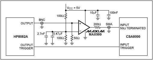
Figure 1. Circuit for measuring the output jitter of the MAX999 comparator
The random jitter of the CSA8000 is specified as 1.0ps RMS (typical value) and 1.5ps RMS (maximum value). The HP8082A pulse generator defines the output jitter as 0.1% of the period + 50ps (peak). Select an output frequency of 80MHz, an output swing of 1VP-P (terminal matching 50Ω), and a center point of 2.5V. By directly connecting the pulse generator to the CSA8000, it can measure jitter of 7.7ps RMS.
When fed into the above input signal, the circuit in Figure 1 can measure the RMS jitter of 11.2ps. Considering the simple structure of the circuit, strict power supply filtering and low EMI environment, it can be assumed that the main jitter introduced by the MAX999 and peripheral components is random jitter.
Assuming that the jitter introduced by the pulse generator is not related to the jitter of the MAX999, the jitter of the latter can be estimated according to Equation 1:
(RJ_PG) ² + (RJ_MAX999) ² = (RJ_MEAS) ² (Formula 1)
Figure 2 provides the parameters of Equation 1.
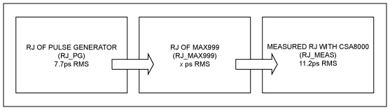
Figure 2. Following this flowchart, the MAX999 jitter can be derived. It is known that the HP8082A pulse generator has 7.7ps RMS, and 11.2ps RMS is measured in the CSA8000, and the jitter of MAX999 is calculated by using Equation 1.
From this formula, it can be determined that the RMS random jitter of the MAX999 is 8.1 ps.
The basic assumption of jitter measurement and error source 8.1ps RMS is an estimate of the actual jitter of MAX999. As mentioned above, this estimate is based on certain assumptions and is affected by the following error sources: 1ps RMS jitter of CSA8000 affects the measurement This leads to 9% uncertainty. Assuming that the jitter of the MAX999 is only related to the random jitter of the thermal noise of the comparator itself and the surrounding resistors, deterministic jitter is ignored. Ignore the noise of two 100Ω resistors that provide 2.5V at the inverting input of MAX999 (0.9nV / ), Assuming that a 7kHz low-pass filter composed of parallel capacitors filters out. Noise generated by 200Ω output series resistance (1.8nV / ) May form another source of error because it is not limited by bandwidth. However, as can be seen from the discussion in the next section, its impact can be ignored compared to the MAX999. The jitter of the HP8082A pulse generator is not related to the jitter of the MAX999. The relationship between jitter and noise Random jitter is caused by the MAX999 and the resistor thermal noise (white noise). Please refer to Application Note 3631: The Effect of Random Noise on Timing Jitter—Theory and Practice to understand the background of random jitter and input white noise interaction in amplifiers. At the switching point, the comparator and amplifier function similarly; in particular, the comparator gain stage causes the output to switch when the two inputs are unbalanced. Application Note 3631 illustrates that the RMS value of random jitter and white noise are related to the input (sinusoidal) signal slew rate, which is expressed by Equation 2:
JitterRMS = VnRMS / SR (Formula 2)
The HP8082A pulse generator has a limited bandwidth, making the 80MHz pulse appear as a sine wave. For a sine wave, Equation 3 gives the slew rate close to the zero crossing:
SR = A × 2 × π × ƒ (Formula 3)
Where A is the amplitude of the sine wave (0.5V or 1VP-P in this example), and ƒ is the frequency (80MHz in this example). This results in a slew rate of approximately 250V / µs = 250µV / ps. Equation 4 can be used to calculate the voltage noise caused by the 80MHz input:
VnRMS = 250µV / ps × 8.1ps = 2025µVRMS (Formula 4)
The noise generated by the 200Ω series resistor in the same bandwidth is 14.3µVRMS and can be ignored. Therefore, the total random noise mainly comes from MAX999 itself.
Conclusion In some applications, a comparator is used to shape the high-speed sinusoidal signal to generate a clock signal. Therefore, it is important to understand the output jitter specifications of the comparator. This application note describes how to derive the output jitter of the MAX999 when using a non-ideal signal generator, and discusses measurement limitations and sources of error. Finally, the relationship between output jitter and input reference voltage noise is obtained.
Introduction to basic jitter theory¹ The Fibre Channel standard defines jitter as “deviation from the theoretical timing of eventsâ€. Jitter fundamentally describes the timing error of the system. It basically has two types: deterministic jitter and random jitter.
Deterministic jitter (DJ) is defined as jitter with a non-Gaussian probability density function. Deterministic jitter appears as a time boundary and has certain causes: duty cycle distortion (caused by the time difference between rising and falling edges), EMI, crosstalk, grounding, and power supply problems. Deterministic jitter is generally expressed by the peak value of the boundary.
Random jitter (RJ) is defined as jitter with a Gaussian probability density function. Random jitter is not limited by the amplitude, and is expressed by the RMS (root mean square) value, which is the standard deviation when the mean is equal to zero. The main source of random jitter is the Gaussian thermal noise (white noise) of system components. For example, in a comparator, thermal noise and slew rate affect each other, producing timing errors at the output switching point.
The sum of deterministic and random jitter or convolution results in total jitter (TJ), which is generally expressed as the measured peak. Converting the RMS value of random jitter to a peak introduces the concept of bit error rate (BER). For the Gaussian probability density function, the peak value theoretically means infinite amplitude. However, by selecting the probability of extreme peaks or the probability of bit errors when the total jitter exceeds the jitter budget, the actual peak can be calculated from the RMS value. For example, peak random jitter less than 10-12 is 14.1 times the RMS value. Table 1 lists the relationship between peak and RMS random jitter and BER.
Table 1. Relationship between peak and RMS random jitter and BER
| Probability of Data Error (BER) | Peak-to-Peak (N × RMS) |
| 10-10 | 12.7 × RMS |
| 10-11 | 13.4 × RMS |
| 10-12 | 14.1 × RMS |
| 10-13 | 14.7 × RMS |
| 10-14 | 15.3 × RMS |
To measure the jitter of MAX999 In some applications, high-speed comparators such as MAX999 are used to shape the input sine wave to generate a clock signal. Since the output jitter of the comparator determines the clock jitter, it is very important to grasp the jitter indicator of the comparator in order to accurately calculate the clock jitter.
This application note uses the circuit shown in Figure 1 to measure the output jitter of the MAX999. Connect the inverting input to a fixed 2.5V reference voltage through a small resistor distribution network, and choose a smaller 100Ω resistor to reduce noise. The non-inverting input is connected to the HP8082A pulse generator through the BNC connector. A 50Ω matching resistor is installed near the non-inverting end.
Connect the MAX999 output to a Tektronix® CSA8000 signal analyzer through a 200Ω series resistor and an SMA connector. The 200Ω series resistance and the 50Ω input impedance of the CSA8000 form a voltage divider network that attenuates the input signal of the CSA8000 to slightly less than 1VP-P. Therefore, the signal is within the maximum input range of the meter. Place a bypass capacitor at the 2.5V reference of the power supply and the inverting input of the comparator.
Figure 1. Circuit for measuring the output jitter of the MAX999 comparator
The random jitter of the CSA8000 is specified as 1.0ps RMS (typical value) and 1.5ps RMS (maximum value). The HP8082A pulse generator defines the output jitter as 0.1% of the period + 50ps (peak). Select an output frequency of 80MHz, an output swing of 1VP-P (terminal matching 50Ω), and a center point of 2.5V. By directly connecting the pulse generator to the CSA8000, it can measure jitter of 7.7ps RMS.
When fed into the above input signal, the circuit in Figure 1 can measure the RMS jitter of 11.2ps. Considering the simple structure of the circuit, strict power supply filtering and low EMI environment, it can be assumed that the main jitter introduced by the MAX999 and peripheral components is random jitter.
Assuming that the jitter introduced by the pulse generator is not related to the jitter of the MAX999, the jitter of the latter can be estimated according to Equation 1:
(RJ_PG) ² + (RJ_MAX999) ² = (RJ_MEAS) ²
(Formula 1) Figure 2 provides the parameters of Equation 1.
Figure 2. Following this flowchart, the MAX999 jitter can be derived. It is known that the HP8082A pulse generator has 7.7ps RMS, and 11.2ps RMS is measured in the CSA8000, and the jitter of MAX999 is calculated by using Equation 1.
From this formula, it can be determined that the RMS random jitter of the MAX999 is 8.1 ps.
The basic assumption of jitter measurement and error source 8.1ps RMS is an estimate of the actual jitter of MAX999. As mentioned above, this estimate is based on certain assumptions and is affected by the following error sources: 1ps RMS jitter of CSA8000 affects the measurement This leads to 9% uncertainty. Assuming that the jitter of the MAX999 is only related to the random jitter of the thermal noise of the comparator itself and the surrounding resistors, deterministic jitter is ignored. Ignore the noise of two 100Ω resistors that provide 2.5V at the inverting input of MAX999 (0.9nV /
), Assuming that a 7kHz low-pass filter composed of parallel capacitors filters out. Noise generated by 200Ω output series resistance (1.8nV / ) May form another source of error because it is not limited by bandwidth. However, as can be seen from the discussion in the next section, its impact can be ignored compared to the MAX999. The jitter of the HP8082A pulse generator is not related to the jitter of the MAX999. The relationship between jitter and noise Random jitter is caused by the MAX999 and the resistor thermal noise (white noise). Please refer to Application Note 3631: The Effect of Random Noise on Timing Jitter—Theory and Practice to understand the background of random jitter and input white noise interaction in amplifiers. At the switching point, the comparator and amplifier function similarly; in particular, the comparator gain stage causes the output to switch when the two inputs are unbalanced. Application Note 3631 illustrates that the RMS value of random jitter and white noise are related to the input (sinusoidal) signal slew rate, which is expressed by Equation 2: JitterRMS = VnRMS / SR
(Formula 2) The HP8082A pulse generator has a limited bandwidth, making the 80MHz pulse appear as a sine wave. For a sine wave, Equation 3 gives the slew rate close to the zero crossing:
SR = A × 2 × π × ƒ
(Formula 3) Where A is the amplitude of the sine wave (0.5V or 1VP-P in this example), and ƒ is the frequency (80MHz in this example). This results in a slew rate of approximately 250V / µs = 250µV / ps. Equation 4 can be used to calculate the voltage noise caused by the 80MHz input:
VnRMS = 250µV / ps × 8.1ps = 2025µVRMS
(Formula 4) The noise generated by the 200Ω series resistor in the same bandwidth is 14.3µVRMS and can be ignored. Therefore, the total random noise mainly comes from MAX999 itself.
Conclusion In some applications, a comparator is used to shape the high-speed sinusoidal signal to generate a clock signal. Therefore, it is important to understand the output jitter specifications of the comparator. This application note describes how to derive the output jitter of the MAX999 when using a non-ideal signal generator, and discusses measurement limitations and sources of error. Finally, the relationship between output jitter and input reference voltage noise is obtained.
Speaker System,Home Sound System,Indoor Speaker System,Outdoor Speakers System
The ASI Audio Technology Co., Ltd , https://www.asi-sound.com