Conventional digital phase-locked loop designs are structurally desirable to achieve stable oscillation control data by employing loop filtering with low-pass characteristics. However, in digital phase-locked loop systems based on digital logic circuit design, it is more difficult to implement low-pass filtering using logic algorithms. Thus, some pulse sequence low pass filter counting circuits have appeared, the most common of which is the "N prior to M" loop filter. These circuits obtain the oscillation control parameters of the controllable oscillator module by counting the phase error pulses generated by the phase detector module. The low-pass filtering counting method of pulse sequence is a relatively complicated nonlinear processing process, and it is difficult to perform linear approximation. Therefore, the system transfer function analysis method cannot be used to determine the design parameters in the phase-locked loop, and the phase-locking performance is further analyzed. In the design method, VHDL language or Verilog HDL language programming is used to complete the system design, and EDA software is used to simulate the system timing to verify the correctness of the design. This design method requires the designer to have a certain understanding of the FPGA hardware, and has a solid hardware description language programming foundation.
In this paper, a loop filter based on proportional integral (PI) control algorithm is applied to the bandwidth-adaptive all-digital phase-locked loop. The mathematical model of the phase-locked loop is established and the performance indexes of the phase-locked loop are analyzed. Relationship with design parameters. Using DSP Builder, the obtained phase-locked loop mathematical model is directly modeled in Matlab/Simulink environment, and computer simulation is carried out. At the same time, the established model file is converted into VHDL program code, and simulation verification is performed in Quartus II software. And use FPGA to achieve.
1 Theoretical analysis of bandwidth adaptive all-digital phase-locked loop
1.1 Theoretical analysis of analog phase-locked loop based on PI control The phase- locked loop is a negative feedback system, mainly consisting of three parts: phase detector (PD), loop filter (LF) and voltage controlled oscillator (VCO). composition. The role of the phase detector is to calculate the phase error between the input signal and the output signal. The main function of the loop filter is to suppress noise and high frequency components, and to control the speed and accuracy of loop phase correction. In order to improve the performance of the phase-locked system, this paper adopts a first-order low-pass filter based on PI control algorithm, which is to multiply the phase error identified by the phase-detection module by a certain proportional coefficient to generate a proportional control parameter and phase error. The size is integrated, and an integral control parameter is generated under the adjustment of the integral coefficient, and finally the sum of the proportional and integral control parameters is taken as the control parameter of the link. The role of the voltage controlled oscillator is to control the frequency of the output signal using the input voltage value. Let the input signal of the voltage controlled oscillator be V0(t), and the frequency of the output signal be ω0+KV0(t), then the phase of the output signal: ![]()
In the formula: ![]() The transfer function of the voltage controlled oscillator is: HVCO(s) = θf(s) / V0(t) = K / s, it can be seen that the voltage controlled oscillator is equivalent to an inherent integral link. In this design, the gain of the voltage-controlled oscillator is K=1, and the block diagram of the analog phase-locked loop based on the PI control algorithm can be obtained by the above analysis.
The transfer function of the voltage controlled oscillator is: HVCO(s) = θf(s) / V0(t) = K / s, it can be seen that the voltage controlled oscillator is equivalent to an inherent integral link. In this design, the gain of the voltage-controlled oscillator is K=1, and the block diagram of the analog phase-locked loop based on the PI control algorithm can be obtained by the above analysis.
This article refers to the address: http://
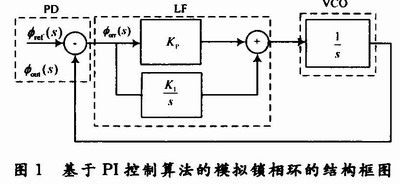
It can be concluded from Figure 1 that the closed-loop transfer function of the phase-locked loop is: ![]()
It is not difficult to see that the system is a typical second-order system, then the closed-loop transfer function of the second-order analog phase-locked loop can be expressed as: 
Where: Kp and Kl are the proportional coefficient and the integral coefficient, respectively. ![]() The natural frequency of the system; ζ is the damping coefficient of the system.
The natural frequency of the system; ζ is the damping coefficient of the system.
1.2 Theoretical analysis of bandwidth adaptive all-digital phase-locked loop The s-domain transfer function of the above-mentioned analog phase-locked loop is discretized. The closed-loop transfer function of the all-digital phase-locked loop is obtained by using the impulse response invariant method: 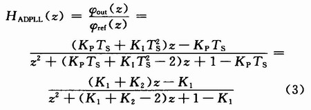
Thus, a structural diagram of an all-digital phase-locked loop based on parameters K1 and K2 can be obtained as shown in FIG. 2.

The two parameters K1 and K2 obtained in equation (5) are analyzed. If c and ζ are constant, the changes of parameters K1 and K2 are only related to the change of the input signal frequency ωref. Therefore, the obtained all-digital phase-locked loop The model has adaptive features, which are new features not found in traditional all-digital phase-locked loops.
2 Bandwidth adaptive full digital phase-locked loop DSP Builder modeling
2.1 DSP Builder Introduction Due to the wide application of FPGA, EDA software QuartusII is particularly important in many fields. At present, the design of all-digital phase-locked loop is mostly completed by EDA technology and realized by FPGA. This requires the designer to be familiar with the FPGA hardware circuit and the hardware description language VHDL or Verilog HDL. At the same time, it is quite cumbersome to use the hardware description language to program the system module in the Quartus II environment. Matlab is powerful in building mathematical models of the system. It has a special modeling and simulation tool Simulink, which can be used for graphical modeling and simulation. However, Matlab itself does not support hardware circuits, and can only perform modeling and simulation of simple mathematical models. If the advantages of the two are combined to make the two strengths and avoid weaknesses, the design of complex electronic systems can be made relatively easy and intuitive.
DSP Builder is a system tool developed by Altera Corporation for DSP development. It appears as a Simulink toolbox from Matlab and can be graphically modeled and simulated in the atlab/Simulink environment. The modules in DSP Builder are presented in an algorithm-level description, which is easy for users to model from the system or algorithm level, and does not even need to fully understand the FPGA itself and the hardware description language. Matlab and Quartus II interface module Signal Compiler are also provided in the module library of DSPBuilder. This module can be used to easily convert the algorithm or system level model established in Ma-tlab/Simulink environment into FPGA compilable suffix. Vhd's VHDL language program. Open the project file in QuartusII, you can compile and simulate the generated program. After the completion, you can lock the pin with the pin condition of the FPGA development board. After compiling and adapting, you can download it to the FPGA development board to complete the hardware test. And hardware implementation.
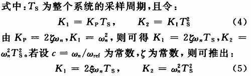
2.2 Bandwidth adaptive DSP Builder modeling of all-digital phase-locked loop This design method is to use Matlab/Simulink environment to establish the mathematical model of the all-digital phase-locked loop obtained by the above analysis in a simple, convenient and fast way. The modeling block diagram is shown in Figure 3. According to the block diagrams of the above modules, the whole system model is formed, and the system clock Clock module and the Signal Compiler module are added to complete the whole system. DSP Builder modeling. The input signals K1 and K2 are calculated by the equation (5) and represented by 6-bit unsigned integers. K1 and K2 can be adaptively adjusted according to the change of the frequency of the input signal Phi_ref; Phi_ref and Phi_out are loops respectively. The input and output signals are represented by a 1-bit unsigned integer.
3 Software Simulation and FPGA Implementation of Bandwidth Adaptive Digital Phase Locked Loop
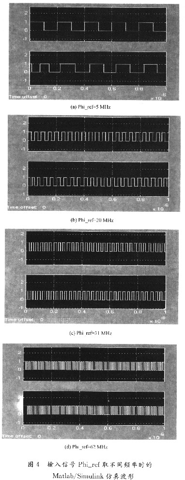
3.1 Bandwidth adaptive software simulation of all-digital phase-locked loop Based on the model established in Figure 3, the software first simulates the bandwidth-adaptive all-digital phase-locked loop, including Matlab/Simulink simulation and Quartus II timing simulation. . The parameters of the system are: damping coefficient ζ=O. 707, system clock period Tclk = 1 / fs, sampling frequency fs = 250 MHz. Figure 4 shows the Matlab/Simulink simulation waveform when the input signal Phi_ref takes different frequencies.
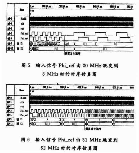
The all-digital phase-locked loop model established in Figure 3 is converted to VHDL language code using the Signal Compiler module in the DSP Builder library. The design completes the overall timing simulation of the bandwidth adaptive full digital phase-locked loop through the Quartus II software. Figure 5 shows the timing simulation of the input signal Phi_ref from 20 MHz to 5 MHz. Figure 6 shows the timing simulation of the input signal Phi_ref from 31 MHz to 62 MHz. Through the Matlab/Simu-link simulation and Quartus II timing simulation of the designed digital phase-locked loop, it can be seen that the system can realize the function of frequency-locking; at the same time, the system has adaptive characteristics, and the input signal has a large variation range. It has good performance inside; finally, the system also has good tracking performance for input signals with frequency jumps.
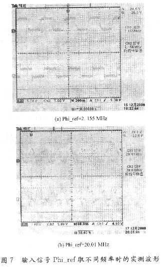
3.2 FPGA implementation and hardware test Because the Signal Compiler module can automatically convert the model file created by DSPbuilder into the project file in the QuartusII environment, the design is combined with the FPGA test box after the software simulation is completed, and the generated project is performed. The pin lock and compile adaptation are downloaded to the FPGA chip to implement the designed bandwidth adaptive full digital phase-locked loop and complete the hardware test. In the hardware test, a signal generator and an oscilloscope are needed. The signal generator is used to generate an input test signal of the phase locked loop, and the oscilloscope is used to observe the input/output waveform of the phase locked loop. Fig. 7 is a measured waveform when the input signal Phi_ref takes different frequencies.
The above software simulation and hardware test show that the designed bandwidth adaptive full digital phase-locked loop system can realize the function of frequency-locking, and the design is successful and feasible.
4 Conclusion This article uses DSP Builder to establish a system model to complete the design of the all-digital phase-locked loop. The theoretical analysis and simulation results are basically the same. It can be seen from the above design process that the DSP-based Buil-der completes the design of the all-digital phase-locked loop, enabling designers to use Simulink's fast and flexible modeling and simulation functions and Matlab's powerful data analysis capabilities for FPGA system-level modeling. Simulation, and liberate designers from the tedious work of writing VHDL or Verilog HDL code language, and focus on building system models under Matlab/Simulink, shortening the design cycle and improving design flexibility.
MOSO Public LED lighting Driver is a IP67,
constant current design for Public lighting application like street light,
tunnel light, Flood light, Stadium Light, etc. This Public LED lighting Driver
has brilliant waterproof design and universal input voltage range that ensure
this LED control gear to be suitable for all of outdoor application use.


The Public Lighting LED Driver got global safety certifications, including UL, CE, TUV, CB, ENEC,SAA, BIS, KC, PSE, etc. The LED Driver has universal input voltage, from 90~305Vac. It is a reliable product compatible with various application and different countries.
The high efficiency of these Public lighting LED Power Supply and compact metal case enable them to run cooler, significantly improving reliability and extend product lifetime to at least 50,000hours.
To ensure trouble-free operation, protection is provided against built-in Surge protection, output over voltage, short circuit, and over temperature.
MOSO grants the product with 5 years global warranty. Customer can refer to Warranty policy, find the closest MOSO distributors or sales representatives, to get a local replacement in case of any failure.
Public Lighting LED Driver
Public Lighting LED Driver,LED flood Light Driver,Outdoor Waterproof Lighting LED Driver,Professional Public Lighting LED Driver
Moso Electronics , http://www.mosoleddriver.com