The miniaturization and low power consumption of wearable devices are common pain points for manufacturers who are engaged in the development of wearable products and satisfying the end user experience. Among the many “small and beautiful†solutions, why is SiP (system-in-package) popular with first-line terminal brands such as Apple? What are the biggest advantages of the solution providers with SiP technology strength for traditional solution providers? The following will look at the new breakthroughs in the wearable industry from the perspective of market demand and corresponding SiP technical solutions and cases.
SiP
SiP (System in Package) system-in-package refers to the use of semiconductor packaging technology to reduce components, packages, and system boards into a single package, minimizing product size. SiP provides better electrical signal transmission characteristics, reduces transmission loss, and reduces system power consumption.
Wearable market with tens of millions of shipments: smaller, lighter, thinner is just needed
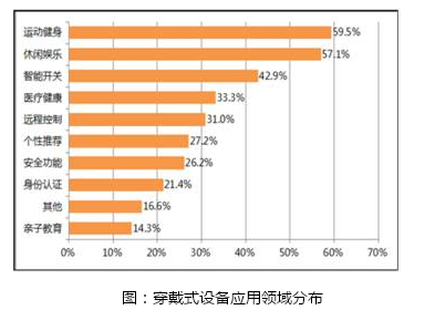
According to the "Smart Product Circle" 2015 China Smart Wearable Industry Report, the global market for wearable products such as smart watches, bracelets, glasses and shoes was 76.10 million units in 2015, with a compound annual growth rate of 22.9%; special Chinese wearables. The market retail volume increased from 4.3 million units in 2014 to 16.8 million units in 2015, which is growing faster than the global level.
High performance, versatility, miniaturization, thinness, portability, and low cost have become common requirements for wearable device developers to achieve end-user experience and product development. How to meet the versatility and high integration while Can the product be smaller, lighter and thinner? Generally, it can be started from three aspects: making the circuit the surface of the industrial design shell, making full use of the structure to save space; selecting small devices, high integration single-chip SoC; and multi-chip system packaging technology SiP. How do SiP win in three ways? The following will take a closer look at the technical characteristics and actual cases.
SiP stands out: three advantages to help you achieve "small and beautiful" product design
1.SiP replaces PCB to solve size problem
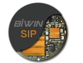
From the perspective of packaging, SiP can simultaneously coordinate small size and cost issues, saving space, increasing fault tolerance, and solving problems such as bad rate/virtual soldering. Apple's smart watch S1 processor encapsulates CPU, Bluetooth, WIFI, NFC, storage and other functional chips into a small single chip through SiP, which opens up the trend of system packaging, such as the Bluetooth intelligent system chip launched by Weiwei BIWIN. The Bluetooth main control, 3-axis accelerometer, two crystal oscillators, memory chips, and power management chips are integrated in a small size of 12mm*9mm.
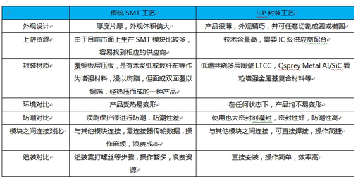
2. SiP three-proof features are not picky about the environment
Industry and industry, especially some special industries such as military industry, have strict industry standards for waterproof, moisture-proof and shock-proof in the application environment and use scenarios; wearable from smart watches, bracelets, smart shoes, smart clothing, and its service life It will vary depending on the environment in which it is used. In order to solve this problem, ordinary electronic products usually use SMT patches on the PCB board. The violent vibration will cause the components or solder joints to fall off. The humid climate will cause the components in the soldering board to corrode and rust, while the products in SiP package. The internal components will not change due to external changes. At the same time, the chip is encapsulated in epoxy resin, which has various characteristics such as wear resistance, anti-corrosion/acid-base/ultraviolet/water/dust/crack, suitable for various complicated and bad. surroundings.

SiP packaging technology advantages
Achieve more compact products
Shorten the cycle of product development and launch
Reduce system cost
Better resistance to mechanical and chemical corrosion
Higher reliability, etc.
3. SiP balances cost, development cycle and performance
Traditional PCBs are difficult to control in terms of thickness and electrical parameters, and the SiP package substrate process can effectively control each parameter to maximize system performance and maintain consistency. On the other hand, although the SiP multi-chip has no advantage over the SoC single-chip from the cost of the die, the overall design difficulty, process cost and manufacturing cycle, the SiP threshold is lower, and even the passive components that the SoC can't do can be used. The antenna, etc. are integrated and the system is more complete.
One-stop SiP solution provider: Promote customized, miniaturized smart product upgrades
The many advantages of SiP package make it quickly applied to module solutions such as communication module, RF module, AP+ communication, and even all components are packaged into product form through SiP. Shenzhen Weiwei Storage Technology Co., Ltd. (abbreviated as: BIWIN) is one of the few semiconductor packaging manufacturers in South China. Since its establishment, it has been committed to developing high-performance, high-reliability microelectronic products. Relying on years of experience in semiconductor package design, three-dimensional packaging technology and chip testing, the company will focus on high-density, high-complexity SiP technology research and development and industrial transformation, with IC design, packaging, testing, assembly and other stations. The service promotes customized and miniaturized intelligent product upgrades. At present, the BIWIN SiP module solution includes smart watch module, Bluetooth intelligent module and wireless charging module.
On April 28th, Weiwei BIWIN will hold the “SSD New Product Launch Conference of the Weiwei SiP Packaging Technology Promotion Conference Wing System†held in Shenzhen, starting from the mainstream industry trends and pain points, and inviting Shenzhen IC R&D Center leaders and industry partners. Let's talk about the application of SiP packaging technology in the industry, and experience the performance experience of the new wing series SSD collection SiP packaging solution in extreme environments.
Usb Charger Cable advantage:
For iPhone Cable Charger High Quality Usb Data Line 2.1A Fast Charging USB Cable For Apple Charging Chord For phones Charger
100% Brand new and high quality.Feel smooth, tough and durable,Original quality cable for smart phone.Set bracket, lightning charging solid data line, copper wire specifications, charging 2 core *25*0.1, data 2 core *12*0.1 74 copper wire.

Usb Charger Cable,Usb Charging Cable,Usb Cable Charging Cable,Micro Usb Charger Cable
Dongguan City Leya Electronic Technology Co. Ltd , https://www.dgleya.com