1. Introduction LED modules are widely used in electronic related products today. With the expansion of application range and the continuous improvement of lighting systems, the demand for high power has increased rapidly since 1990, especially in the case of white light and high power type. The LED power used in the current lighting system has not only 1W, 3W, 5W or even more than 10W, so the heat dissipation performance of the heat dissipation substrate has become the most important issue. The main factors affecting LED heat dissipation include the material and design of LED chip, chip carrier, chip package and module, and the accumulated thermal energy of LED and its package materials are mostly transmitted in conduction, so LED chip substrate and The design and material of the LED chip package has become the main key.
2, the impact of the heat sink substrate on the LED module
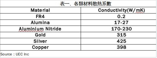
LEDs have seen red LEDs since 1970, and have since evolved into blue and green light. The initial use is mostly on some labels, such as indications on household appliances, and since 2000, white high-power LEDs have been used. Appeared, let the use of LEDs begin to enter another stage, such as outdoor large-view version, backlight of small display, etc. (Figure 1), but with the rapid evolution of high power, it is expected that after 2010, automotive lighting, The demand for indoor and special lighting is increasing, but the requirements for heat dissipation of these high-power lighting devices are becoming more stringent. Because ceramic substrates have high heat dissipation capability and high heat resistance and air tightness, The ceramic substrate is one of the most commonly used substrate materials for high-power LEDs.
However, the most common ceramic substrates currently on the market are ceramic heat-dissipating substrates made of LTCC or thick film technology. This type of product is subject to the bottleneck of screen printing technology, which makes it impossible to match the higher-order welding. , Eutectic or Flip chip packaging, and the ceramic thermal substrate developed by the thin film process technology provides high alignment accuracy products in response to the development of packaging technology.
2.1, the choice of heat sink substrate
In terms of the development of the LED chip carrier substrate, the substrate material of the conventional PCB has a highly commercial feature in terms of carrying the chip, and has considerable influence in the initial stage of LED development. However, with the increase of LED power, the heat dissipation capability of the LED substrate has become one of its important material properties. For this reason, the ceramic substrate has gradually become the main heat-dissipating substrate material for high-performance LEDs (as shown in Table 1), and gradually Accepted by the market and widely used. In recent years, in addition to the material properties of the ceramic substrate itself, the requirements for the line width, wire diameter, metal surface flatness and adhesion of the metal lines on the substrate are increasing, so that the ceramics prepared by the conventional thick film process are required. The substrate is gradually used, and a thin film type ceramic heat dissipation substrate has been developed. This paper will analyze the difference between the thick film and the film process and the product characteristics of the ceramic heat dissipation substrate.
3, ceramic heat sink substrate
From traditional PCB (FR4) boards to ceramic substrates, LEDs are constantly evolving to higher power requirements. At this stage, the metal lines of ceramic substrates are mostly formed by thick film technology. However, the alignment accuracy of thick film printing makes it Can not keep up with the progress of LED packaging technology, the main factor is the use of eutectic and flip chip packaging technology in the heat dissipation design of higher power LED components, the introduction of these technologies can not only use high luminous efficiency LED chips, It can also greatly reduce its thermal resistance value and make the joint degree more perfect, so that the power of the overall operation is relatively improved. However, the application of these two bonding methods requires the basis of accurate metal circuit design. Therefore, the thin film ceramic heat dissipation substrate with the exposure lithography as the alignment mode becomes the mainstream of the precision circuit design.