The image input system front-end input signals currently used are generally standard full-TV signals of the PAL system, one frame every 20 ms, every 40 ms. After the analog signal is converted into a 720×576 digital signal by the video decoder, the target is segmented, identified and tracked, and the position angle deviation of the target is accurately calculated and transmitted to the servo mechanism. In a system, it is required to accurately track a small target of 3×3 pixels. In order to achieve tracking accuracy, the frame rate of image input can be improved and the resolution of image input can be improved. Therefore, the front end adopts a camera based on DALSA. A digital camera with a Link interface that has a frame rate of 100 Hz and a resolution of up to 1 400 × 1,024. In this way, the frame processing time is only 10 ms. Considering the real-time performance of the system, we use TI's high-performance DSP chip TMS320C6414 and high-performance FPGA chip EP2S30F672 as the core hardware processing platform.
This article refers to the address: http://
1 system hardware structure and working principle
The structure of the whole image tracking module is shown in the dotted line in Figure 1. The whole system includes an image acquisition and preprocessing unit with FPGA as the core, an image processing unit with DSP as the core and an image display unit controlled by FPGA.
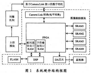
Since the storage, processing, and display all need to access the memory, in order to reduce the cost, the ordinary asynchronous SRAM is used. According to the function, it can be divided into SRAM group for acquisition processing and SRAM group for acquisition display. Each group includes two SRAMs respectively. The read and write logic is controlled by FPGA and switched by ping-pong method.
For the acquisition processing part, in the Kth frame, SRAM1 is controlled by the FPGA to write the image data, while SRAM2 is processed by the DSP reading; in the K+1th frame, the SRAM2 is controlled by the FPGA to write the image data, and the SRAM1 is read by the DSP. Process it.
For the acquisition display part, in the Kth frame, the SRAM3 is controlled by the FPGA to write the image data, while the SRAM4 is displayed by the FPGA reading; in the K+1th frame, the SRAM4 is controlled by the FPGA to write the image data, and the SRAM3 is read by the FPGA. Display.
The whole system works like this: the image acquisition unit becomes an LVTTL signal via a differential conversion chip, and is directly connected to the FPGA. The FPGA controls the digital image acquisition, and after image preprocessing, the image data is stored in the SRAM. An interrupt signal is sent to the DSP. After the DSP responds to the interrupt, after reading one frame of image data from the SRAM, image segmentation, target extraction, and target tracking algorithms are performed, and the azimuth and elevation angle deviation components are calculated, and the result is passed through the on-chip of the FPGA. The inter-board communication dual-port RAM is transmitted to the main control module, and the main control module adjusts the servo mechanism to ensure that the tracked target is in the center of the field of view.
The main control module can also transmit some state variables of the system to the DSP through the inter-board communication dual-port RAM in real time. The DSP generates characters to be displayed according to these states, and writes these characters into the FPGA-on-character superimposed dual-port RAM. The FPGA reads the image data in the display RAM and the data in the on-chip character superimposition dual-port RAM, superimposes the crosshairs and the wave gate on the original image, and some state character information of the system, and sends the video data to the DA chip according to the PAL system timing. This allows the monitor to output a standard PAL image.
2 individual unit design
2.1 Image acquisition and preprocessing unit based on Camera Link interface
Camera Link is an interface developed based on video applications that solves the problem of speed matching between video data output and acquisition. The transmission rate of Camera Link data is very high, up to 1 Gb/s, and the LVDS format is adopted, and the anti-noise performance is good. Camera Link's signal consists of three parts: the serial communication part, the camera control part, and the video signal part. The detailed picture acquisition unit based on the Camera Link interface is shown in Figure 2. Each part uses a special differential conversion chip. The serial communication section converts the asynchronous serial port to a standard RS 232 level, which allows the master to adjust the camera's exposure time, contrast, and other settings. The camera control section includes four pairs of differential signals for controlling the camera, such as the camera's external sync signal input control, which can be controlled by the FPGA. The 28 b LVTTL signal in the video section is the key control part. They are directly connected to the FPGA, and the FPGA controls the timing of the acquisition.
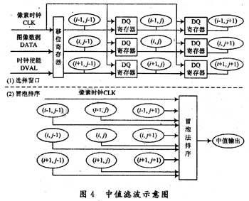
The 28 b data includes 3 data ports: A port (8 b), B port (8 b), C port (8 b), and 4 video control signals FVAL (frame valid), DVAL (data valid), LVAL (line valid), SPARE (empty, temporarily unused). As for the clock signal converted by the Camera Link chip, it is the synchronous driving signal of the entire camera, and all the data and video control signals are synchronized with the clock signal, and the timing chart of the camera is shown in FIG.
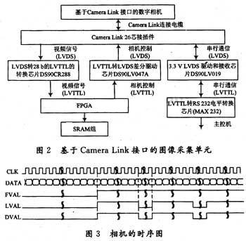
The camera can be configured for 8 b or 10 b output bit width, 40 MHz pixel clock or 80 MHz pixel clock, 2 x 40 MHz or 2 x 80 MHz data output rate. Regarding the logic code of the Camera Link acquisition data, the key point is to generate the address signal of the memory, the memory write signal, and stably write the data into the memory at the corresponding address. We use the pixel clock to generate the column address counter, and the row sync signal generates a row address counter, which is spliced ​​to generate the address signal of the memory. The effective address thus generated is not continuous, but has a clear meaning and is advantageous for displaying the interlaced interlace of the display portion. For 8 b data, 4 valid data can be spliced ​​into 32 b and then stored, which can reduce the speed of FPGA reading and writing memory.
2.2 FPGA-based image preprocessing unit
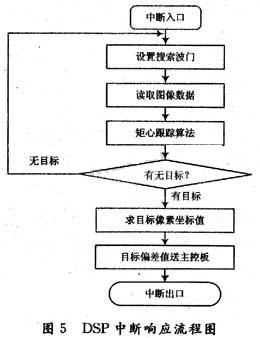
Aiming at the simple operation structure of the image preprocessing stage, hardware implementation with FPGA is undoubtedly an ideal choice, which simultaneously considers the speed and flexibility, and greatly reduces the burden on the DSP. The preprocessing algorithm used here is mainly median filtering. The median filter is a nonlinear filter. Compared with the mean filter and other similar filters, the median filter has the ability to completely filter out the spike interference. At the same time, the noise can better protect the edge of the target image. The specific implementation process of median filtering is generally:
(1) Select an n × n sliding window (usually 3 × 3 or 5 × 5) to slide it pixel by pixel along the row or column direction of the image data (usually from left to right, top to bottom progressive) mobile).
(2) After each sliding, sort the grayscale values ​​of the pixels in the window, and replace the grayscale values ​​of the pixels in the center of the window with the intermediate values ​​obtained by the sorting.
Realizing two-dimensional median filtering in hardware, it is important to reliably store real-time image data with minimal latency. The processing starts after storing n-1 lines of image data, where n is the window size. In this design, the median filter of 3*3 window is selected, that is, n=3. The advantage of this design is that the FPGA can implement the module in serial pipeline mode, saving a lot of time and creating favorable conditions for real-time processing.
In order to save resources as much as possible, and make full use of the "module reuse" principle in hardware design, we need to design a shift register, a dq register, a binary comparator, and then, under the driving of the pixel clock, first call the shift. The register and dq registers generate window data, and then call the dq register and the 2-value comparator multiple times on the data in the 3×3 template for bubble sorting to output the intermediate value. The schematic diagram of the median filter module is shown in Figure 4.
2.3 DSP-based image processing unit
TI's TMS320C6414 chip is a high-performance fixed-point DSP processor with a clock speed of up to 720 MHz, on-chip rich RAM resources, and many memory chips can be expanded through EMIFA and EMIFB ports. The main extension here is the program FLASH chip, which is used to store the cured program code.
I have already explained how the FPGA controls the SRAM read and write logic. The main work of the DSP is to respond to the interrupt signal sent by the FPGA and read the image data for processing. Although the actual SRAM read by each frame is different, after mapping through the FPGA. For the DSP, the SRAM is always in the fixed address range at the end of the DSP chip. The flowchart of the DSP response interrupt is shown in Figure 5.
Taking the commonly used simplest centroid tracking algorithm as an example, after each response of the DSP, the main work is: first set the search gate, and quickly move the data in the gate to the on-chip memory through DMA. Then, it is processed by the centroid tracking algorithm until the target is searched, and the position deviation of the target pixel is calculated and sent to the main control board.
2.4 FPGA-based image display unit
The system requires the output of the standard PAL analog video. Since the PAL video has a field frequency of 50 Hz and a frame rate of 25 Hz, the digital image of the front-end high-resolution and high-frame rate must be down-converted and the resolution must be reduce. The dedicated image DA chip ADV7123 is used. The input bit width is 10 b, and the data rate that can be converted can reach 240 MHz. Because the standard PAL video can only display 576 lines of valid lines in one frame, only 512 lines can be displayed interlaced for the data image of 1,024 lines, and 256 lines of odd fields and 256 lines of even fields. Therefore, for the acquired image, the resolution is reduced in the row direction, but the resolution is not lowered in the direction of the column.
As can be seen from the foregoing, since the acquisition display adopts the ping-pong structure, since the display is displayed by the interlaced snapshot, and the displayed frequency frame rate is 25 Hz, the data storage should be taken alternately in the acquisition part, and updated every 2 frames. Data collected. Unlike the acquisition processing section, the acquired data is updated every frame.
The clock signal, composite sync signal, and composite blanking signal that control the ADV7123 are generated by the FPGA. The line, field sync and blanking signals associated with television are the key to PAL analog video signal generation.
After the FPGA multiplies the 80 MHz clock down to the digital camera, the clock counts and logically combines the operations to obtain the same variety. Step timing signal. The clock signal of the ADV7123 is divided by 2 times the frequency of the 80 MHz clock and then divided by 5, that is, the pixel clock frequency is 32 MHz and the period is 31.25 ns. The resulting image size is 1 400 x 576 pixels, which means 288 lines per field and 1 400 pixels per line. The system adopts PAL interlaced scanning mode with a field period of 20 ms and a line period of 64 μs, so each field contains 312.5 line periods, but the high level of the field blanking lasts for 288 line periods, as long as the field blanking signal is adjusted. The starting position makes it easy to have the output of the video image in the middle of the screen. The implementation of the line sync signal and the blanking signal is basically the same: counting the clock, when counting a certain value, turning the output signal (from low level to high level or high level to low level) The period of the counter and the period of the flip vary depending on different parameters. Since these timings are programmed in the FPGA, they are easy to adjust and modify.
As for the character superposition process, the DSP writes the character dot matrix to be superimposed in the FPGA on-chip dual-port RAM according to the position and size of the actually superimposed characters on the image (the binary character 1 is written in the place where the character is displayed, and the binary image is written in the place where the image is displayed. 0), display each frame of the output, the FPGA reads the character superimposed dual-port RAM, and determines whether to output the captured image or output the superimposed character according to its value. In this way, through the cooperation of DSP and FPGA, any character can be flexibly superimposed, and the DSP can change the value in the character overlay RAM according to any state change of the system, thus ensuring that the system has a good human-computer interaction interface.
3 Conclusion
Taking high-performance DSP and FPGA as the core, the digital camera of Camera Link interface is used for image acquisition, and a real-time image tracking system is established by digital image processing technology. The system is small in size, light in weight, high in reliability, and has a good human-computer interaction interface, which has been successfully applied in practical projects.
Plug Adapter,Mini Plug Socket,Mini Travel Plug
Double USB Travel Plug,Single Country Plug Adapter Co., Ltd. , http://www.chtravelplug.com