Every chip that operates under real-world conditions must function within a specific temperature range, which is typically measured at the silicon junction—known as the junction temperature. This parameter is critical because it directly affects the reliability and performance of the device.
Altera's FPGAs are categorized into commercial and industrial grades. Commercial-grade chips can operate between 0°C and 85°C, while industrial-grade chips are designed to work in a broader range, from -40°C to 100°C. In practical applications, it's essential to ensure that the junction temperature of the chip remains within its specified limits to avoid thermal damage or malfunction.
As a chip consumes more power, it generates more heat during operation. To keep the junction temperature within safe levels, effective cooling mechanisms must be implemented to transfer the heat away from the chip quickly. This is especially important in high-performance systems where thermal management plays a crucial role in maintaining stability and longevity.
From basic physics, we know that heat transfer occurs through three main methods: conduction, convection, and radiation. Similarly, chip cooling relies on these principles. The most common approach involves using a heat sink, which enhances heat dissipation by increasing the surface area exposed to the air and improving airflow around the component.
The diagram below illustrates a simplified model of chip heat dissipation. The heat generated by the chip is primarily transferred to the package. If no heat sink is attached, the heat spreads directly into the environment through the package. When a heat sink is used, the heat moves from the chip’s package through the heat sink and then dissipates into the surrounding air. Heat sinks are often black because dark surfaces radiate heat more efficiently, and increased airflow over the heat sink improves cooling performance.
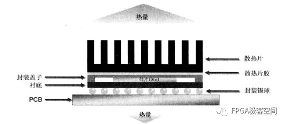
Simplified Chip Heat Flow Model
In addition to conduction through the package, a small portion of the heat may also travel through the chip’s substrate and solder balls, eventually reaching the PCB and dispersing into the environment. However, this path contributes minimally to overall heat dissipation and is usually ignored when calculating the main thermal resistance values of the chip and its packaging.
Understanding the concept of "thermal resistance" is key to analyzing heat dissipation. Thermal resistance measures how effectively an object conducts heat. Lower thermal resistance means better heat transfer, similar to electrical resistance. A lower value indicates a more efficient cooling path.
To simplify the thermal analysis, we consider the total thermal resistance from the silicon junction to the ambient environment, assuming all heat is dissipated through the heat sink. This leads to a basic thermal resistance model, as shown below:
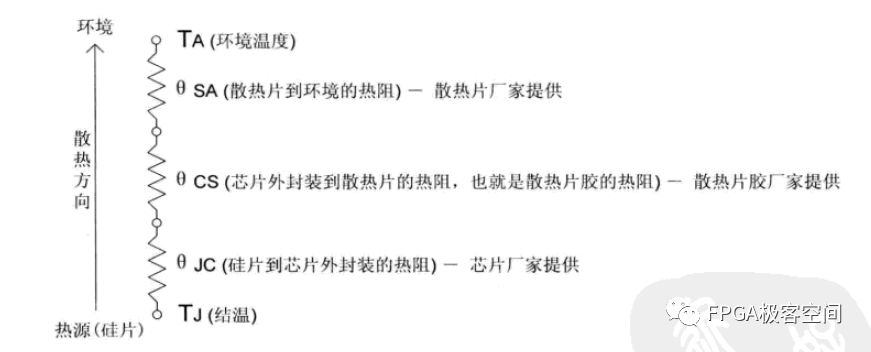
Chip Heat Dissipation Model with Heat Sink
This total resistance is referred to as JA (Junction-to-Ambient). It can be calculated as the sum of three components: JC (Junction-to-Case), CS (Case-to-Sink), and SA (Sink-to-Ambient). JC is provided by the chip manufacturer, CS depends on the thermal interface material used, and SA varies with airflow and is typically given by the heat sink supplier for different wind speeds.
When no heat sink is used, the package itself acts as a passive heat spreader. In this case, the total thermal resistance (JA) is higher compared to when a heat sink is added. This value is influenced by the package design and is usually provided by the chip vendor.
The figure below shows the thermal resistance values for Altera’s Stratix IV devices. These values help determine the junction temperature without a heat sink and are used to calculate the total thermal resistance when a heat sink is applied.
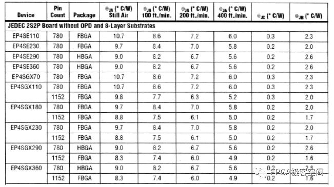
Thermal Resistance in Stratix IV Device Packages
If a chip consumes power P, the junction temperature can be calculated as:
TJ = TA + P × JA
Where TJ is the junction temperature, TA is the ambient temperature, and JA is the total thermal resistance. To ensure safe operation, TJ must not exceed the maximum allowable junction temperature. Using this formula, you can determine the maximum allowable JA value based on the ambient temperature and the actual power consumption of the chip.
JAMax = (TJMax - TA) / P
If the existing JA value of the chip exceeds this limit, it's necessary to add a suitable heat sink to reduce the effective thermal resistance and prevent overheating.
In real systems, some heat may also be dissipated through the printed circuit board (PCB). A multi-layer PCB with a large area can significantly improve heat dissipation, making it an important consideration in thermal design.
Outdoor Cabinet Lock,Cabinet Material,Outdoor Telecom,Electrical Cabinet
Guangdong Yuqiu Intelligent Technology Co.,Ltd , https://www.cntcetltd.com