Every chip that operates under real-world conditions must function within a specific temperature range, known as the junction temperature, which refers to the temperature at the silicon die itself.
Altera’s FPGAs are typically categorized into commercial and industrial grades. Commercial-grade devices are designed to operate between 0°C and 85°C, while industrial-grade ones can handle temperatures from -40°C to 100°C. In practical applications, it is crucial to ensure that the junction temperature of the chip remains within its specified limits to avoid performance issues or failure.
As power consumption increases, so does the heat generated by the chip during operation. To keep the junction temperature within acceptable limits, effective cooling solutions must be implemented to efficiently transfer the heat away from the chip and into the surrounding environment.
Anyone with a basic understanding of middle school physics knows that heat transfer occurs through three main mechanisms: conduction, convection, and radiation. The same principles apply to chip cooling, and various methods are used to manage thermal output effectively.
The diagram below illustrates a simplified model of chip heat dissipation. The heat generated by the chip is primarily transferred to the package. If no heat sink is attached, the package directly transfers the heat to the ambient air. However, when a heat sink is added, the heat moves from the chip's package through the heat sink and then into the environment. Heat sinks are usually designed with a large surface area to maximize heat exchange with the air, making them more efficient. Additionally, most heat sinks are black because dark surfaces radiate heat more effectively. The faster the airflow over the heat sink, the better the cooling performance.
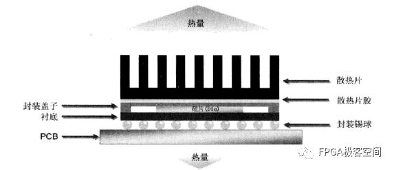
Simplified Chip Heat Flow Model
In addition, a small portion of the heat is conducted through the chip substrate and then via the solder balls to the PCB, eventually dissipating into the environment. However, this path contributes minimally to overall heat dissipation and is often neglected when analyzing the thermal resistance of the chip and heat sink.
To understand how heat is managed in a chip, we first need to grasp the concept of "thermal resistance." Thermal resistance measures how well a material conducts heat. The lower the thermal resistance, the more efficiently heat is transferred—similar to electrical resistance, where lower resistance allows for better current flow.
When considering the entire heat path from the silicon wafer to the environment, we assume that all heat is eventually dissipated through the heat sink. This leads to a simplified thermal resistance model, as shown below:
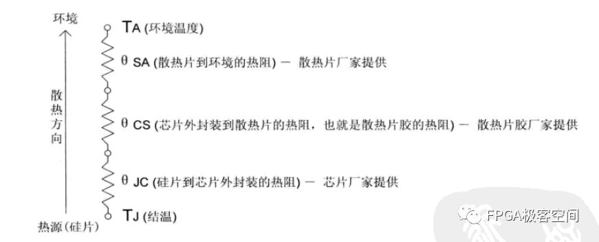
Chip Heat Dissipation Model with Heat Sink
The total thermal resistance from the silicon die to the environment is denoted as JA. It can be calculated as:
JA = JC + CS + SA
Where JC represents the thermal resistance from the chip to its package, typically provided by the manufacturer. CS is the thermal resistance between the package and the heat sink, which depends on the thermal interface material used. SA is the thermal resistance from the heat sink to the environment, which decreases with higher airflow and is usually specified by the heat sink supplier.
If no heat sink is used, the package itself acts as a heat spreader. In this case, the thermal resistance (JA) is higher than when a heat sink is attached. This value is determined by the package design and is provided by the chip manufacturer.
The following figure shows the thermal resistance values for Altera’s Stratix IV device packages. These values help estimate the junction temperature without a heat sink. They also serve as a reference when calculating the total thermal resistance with a heat sink in place.
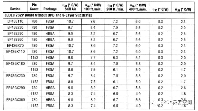
Thermal Resistance in Stratix IV Device Packages
Assuming the chip consumes power P, the junction temperature can be calculated using the formula:
TJ (junction temperature) = TA + P × JA
This temperature must not exceed the maximum junction temperature allowed by the chip. By knowing the ambient temperature and the actual power consumption, we can determine the maximum allowable JA value. If the chip's inherent JA is too high, a suitable heat sink should be added to reduce the effective thermal resistance and prevent overheating.
In real systems, some heat is also dissipated through the PCB. A multi-layer PCB with a large area can significantly improve heat dissipation, especially in high-power applications.
Cabinet Energy Storage,Battery Energy Storage Systems,Solar Energy Solution,Battery Storage
Guangdong Yuqiu Intelligent Technology Co.,Ltd , https://www.cntcetltd.com