The method of using existing 3G mobile communication network to realize wireless video transmission is suitable for long-distance use. The use of this transmission method at short distances is not only expensive, but also the bandwidth is not guaranteed. A short-range wireless video transmission system is designed to solve the above problems. The system uses a special JPEG2000 video compression device ADV212 to achieve video compression; based on the consideration of multiple external interfaces and low power consumption, the embedded processor LPC1768 of the Cortex-M3 core is used to control the entire system; wireless transmission is implemented by nRF24LU1 +.
1 Composition of wireless video transmission system
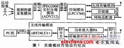
The wireless video transmission system is mainly composed of video image acquisition module, JPEG2000 real-time compression module, control module and communication module. The block diagram of wireless video transmission structure is shown in Figure 1.
The main modules are introduced as follows:
â‘ The video image acquisition module, which is composed of CMOS image sensor OV7670, completes the image acquisition and filtering process;
â‘¡JPEG2000 real-time compression module, mainly real-time compression of video by the JPEG2000 codec chip ADV212;
â‘¢Control module (LPC1768), processing infrared trigger signal and video storage and transmission;
â‘£Communication module, including wireless transmission module and network adapter (expandable);
⑤ memory, SD memory card.
2 System module design
The system mainly includes video image acquisition module, JPEG2000 real-time compression module, control module and wireless transmission module.
2.1 Video image acquisition module
Video image acquisition is completed by OmniVision's OV7670 image sensor, and the JPEG2000 real-time compression module is implemented using Analog Devices' ADV212 real-time compression chip.
2.1.1 OV7670
The OV7670 is a 300,000-pixel CMOS VGA image sensor. It has the characteristics of small size and low working voltage. It can provide all the functions of a single-chip VGA camera and image processor; through the SC CB bus control, it can output various resolutions of 8 bits in the form of full frame, sub-sampling, window acquisition Image data; the highest frame rate can reach 30 fps, users can fully control the image quality, data format and transmission method; all image processing functions such as gamma curve, white balance, saturation, chroma, etc. can be SCCB through the I2C bus Configured in a manner; the photosensitive array is 640x480, and can output YCbCr (4: 2: 2) format data.
2.1.2 ADV212
ADV212 is a special image compression codec chip used by ADI to implement the latest algorithm standard JPEG2000 for static image compression. It uses SRAM process structure, low delay, low power consumption and low cost. The working mode can be flexibly controlled by setting internal registers, which is suitable for the compression processing of various video and still image format data. It is mainly composed of pixel interface, wavelet transform engine, entropy codec, embedded processor, memory system, internal DMA engine and external DMA engine. The single-chip ADV212 can process up to 1 MB of data in a single compression. The YCbCr (4: 2: 2) format is used in the design. The single-frame data volume is 600 KB, which can fully meet the requirements. The block diagram of video image acquisition and control structure is shown in Figure 2.
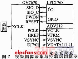
The initial configuration of OV7670 is configured by the controller LPC1768 through the I2C bus in SCCB mode. The register address range that can be read and written is 00 to C9H, many of which do not need to be rewritten, only the default value; The enable signal is DISABLE = 0; the slave address 0x42 is write and 0x43 is read. Commonly used register COM7 (12H) is the output format register, COM10 (15H) is the field setting register and other COM-like general control registers.
LPC1678 makes it go to sleep by setting pin PWDN high. If there is a trigger signal, video image acquisition is performed; video acquisition is done by OV7670 and ADV212. Pin PCLK is the pixel clock signal, HREF is the line synchronization signal, VSYNC is the frame synchronization signal, and the data format is YCbCr (4: 2: 2) (8 bits). This is in line with the format required by the ADV212 chip, and the data transmission is completed through the D [7: 0] pin of the OV7670 and the VDATA [11: 4] pin of the ADV212.
2.2 Wireless transmission module
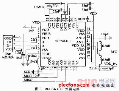
2.2.1 nRF24LU1 + wireless transceiver chip
nRF24LU1 + is a wireless transceiver chip launched by Nordic that combines high-performance RF transceiver and single-chip USBdongle function. It can realize the conversion of wireless data to USB data, so that the connection between the chip and the PC is realized. nRF24LU1 + contains an enhanced 8051 core, wireless transceiver module, and a device controller that meets the full-speed USB 2.0 standard. The operating voltage range of VBUS (USB working power supply) is 4.0 ~ 5.25 V. nRF24LU1 + is a monolithic structure, the overall size is 5 mm & TImes; 5 mm. It has a maximum rate of up to 2 Mbps and is compatible with all nRF24 series chips; using Enhanced Shocked Bust technology can realize the automatic packaging, unpacking and transmission processing (answer / retransmission) of data packets. The nRF24LU1 + peripheral circuit is shown in Figure 3.
LED Flood Light,Hot Selling Flood Light,LED UFO High Bay Light,Solar Panel
Jilin Province Wanhe light Co.,Ltd , https://www.wanhelight.com