Abstract: E-Beam (electron beam) lithography (Lithography) is the next generation of maskless semiconductor process. Through the reticle lithography technology, the lithography process can break through the current limit of 20 nm or less. The E-Beam lithography system requires a very high-bandwidth data transmission system to decompress a large amount of integrated circuit pattern data from the data server through the data transmission system, and then transmit it to the E-Beam machine in parallel through thousands of fibers. The clock skew between channels and channels must not exceed 2 ns. Based on the high channel high density and high data transmission bandwidth requirements, ADLINK uses the AXIe platform architecture to build the E-Beam data transmission system. This article explains how to take full advantage of the features of the AXIe platform to meet the stringent requirements of this thousands of channels of synchronization.
This article refers to the address: http://
Introduction
As mentioned above, E-Beam's reticle-free lithography technology can break through the limitations of traditional reticle lithography. Conceptually like an ultra-high speed printer. Unlike the printer that ejects ink, the E-Beam machine's electron gun projects thousands of parallel electron beams onto the surface of the wafer covered with photoresist. More than 8,000 electron beams pass through the MEMS array to control individual electron beams. The switches, and the control commands for each of the beam switches, are controlled by individual high-speed fiber output channels, which would require more than 8,000 fiber output channels. In order to avoid circuit pattern distortion and errors caused by control commands being out of sync, the overall system requirement is that the clock offset of data between all Fibre Channels cannot exceed 2 ns.
The economically achievable output standard is more than 10 per hour, in other words one wafer is completed every 6 minutes. The data volume of each integrated circuit mask file can be as high as 2.5TB, so another challenge is how to pass large amounts of data through the graphics transmission system in real time, and then output it to the E-Beam machine in parallel through more than 8,000 sets of Fibre Channel. This data is processed by the system and can be used to control the electron beam control array on the E-Beam system. To meet these needs, ADLINK uses an AXIe-based FPGA architecture solution for data processing and storage.
Advantages of AXIe
AXIe is based on the AdvancedTCAR (Advanced Telecommunications Computing Platform) open standard and is a new standard for high-end measurement instruments. Based on the following features of AXIe, this graphics transmission synchronization system chose AXIe as the solution for this system:
· 6U large-size board area, providing enough space to accommodate high-density fiber output channel circuits.
· Provides up to 200 watts of high power per slot.
· A high-performance cooling system is sufficient to solve the heat energy caused by high power consumption.
· High-speed PCIe (PCI Express) bus architecture
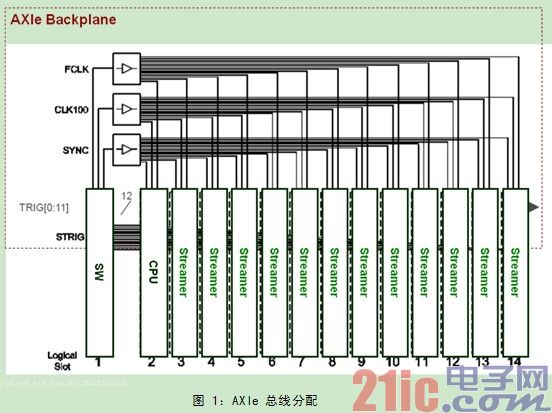
· Highly scalable, a single AXIe chassis can accommodate from 1 to 14 slots, while multiple sets of chassis can form a large number of channels of synchronization.
· Hardware platform management capabilities, including chassis management controllers, intelligent platform management controllers, and hot plugging capabilities.
Synchronization and local bus functions provide the precise frequency required for each slot.
Graphics transport architecture
The graphics transmission system includes a computer module, a PCIe converter module, multiple sets of data transmission modules, a 14-slot AXIe chassis, an external synchronization signal generator, and a disk array (RAID) system, as shown in FIG.
During electron beam printing, the computer module accesses the integrated circuit image file from the data center (ie, the disk array system) to the memory storage on the system through the 6 Gbps SAS interface. The PCIe switch module is located in the hub slot and provides automatic PCIe channel switching. It is responsible for transferring the integrated circuit files stored in the memory to different data transmission modules through the PCIe high-speed data interface. Each transport module can support 72 sets of fiber output channels. The external sync signal generator generates a set of common operating frequencies and trigger signals to allow multiple chassis to operate simultaneously.
Most of AXIe's unique features are used by graphics transmission systems, including: mechanism design and assembly, hardware platform management and monitoring mechanisms, power distribution mechanisms, active cooling systems, and data transfer interfaces.
The E-Beam system chassis is more complex and synchronized, and must use AXIe STRIG and SYNC signals. This ensures that the point trigger system achieves the specified precise and low jitter synchronization of each slot.
Channel-to-channel skew
The hardware design of the E-Beam system ensures that the clock skew between channels is no more than 2ns. Starting from the external sync signal generator, a low-offset fan-out buffer is used in the external sync signal generator as a means of distributing the operating frequency and sync signals to the chassis switching modules. In addition, the switching module not only provides the PCIe bus automatic switching function, but also switches the STRIG, SYNC and related frequency signals, and distributes these synchronization signals to the data transmission modules on each slot. In terms of the data transmission module, in addition to paying special attention to the frequency and data signals on the PCB must use equal path length, the low-impedance buffer is also used in the output part of the circuit. The last processed data will be from the Avago parallel fiber launcher
(AFB-810BHZ-TX) output. After considering the factors such as FPGA internal winding and process, fiber, connector and PCB path, the calculated overall channel-to-channel skew can be less than 1 ns.
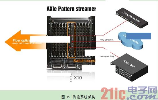
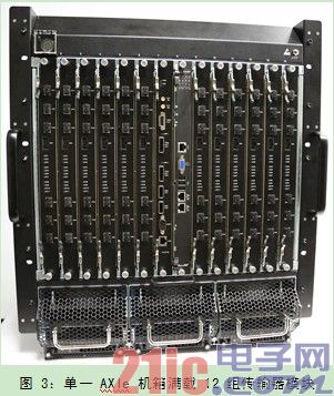
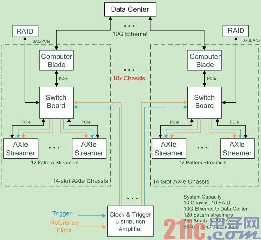
Figure 4: System frequency diagram
High bandwidth graphics transfer
In addition to the strict inter-channel skew requirements across 10 chassis, the system also requires the ability to transfer large amounts of data to the fiber output channel in real time. Each graphics transmission module is equipped with four high-performance FPGAs; one is responsible for the PCIe drive interface, and the other three are responsible for 24 Fibre Channel drive interfaces, that is, a single data transmission module can provide 72 fiber output channels.
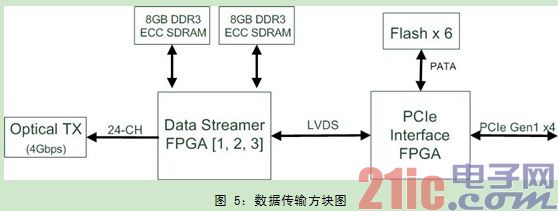
The integrated circuit pattern data is read from the RAID disk array and loaded into the memory of the motherboard blade server, and then transferred to the individual data transmission module via the PCIe bus for direct memory access (DMA). The PCIe FPGA on the data transfer module receives the DMA data and stores it in the flash memory on the module, and then transfers it to the DDR3 memory storage corresponding to each graphics transfer FPGA. The graphics transfer FPGA has a built-in custom decompression algorithm, and the decompressed data is output by the optical transmitter. See Figure 5 for a schematic diagram:
The DDR3 memory is cut into two blocks to implement the "ping-pong" technique, which allows a large amount of data to enter and exit the memory at the same time to optimize the read/write bandwidth. The graphics file size of each fiber output channel can reach 300MB. In other words, a chassis with 12 data transmission modules will require a total file size of about 260GB.
The previously mentioned cost-effective output standard is to complete one wafer every 6 minutes, so overall a continuous data bandwidth of at least 725MB/sec would be required. Through this mode of operation, another completely different wafer schematic file. It can also be downloaded before the pre-wafer fabrication is completed to achieve a small variety of high-performance outputs.
to sum up
ADLINK's FPGA-based AXIe graphics transmission system provides high-efficiency integrated circuit graphics data processing, transmission, and data synchronization solutions for reticle-free E-Beam lithography process applications, and overall system-to-channel clock skew Less than 2ns, and the application of AXIe features, including high power supply, effective heat dissipation and high reliability and expandability, in line with the actual semiconductor manufacturing process needs.
With the continuous development of technology, Led Video Wall has been widely used in various industries. Video wall is very general, suitable for any application and environment.
LED video wall makes use of multi-media technology, computer technology, video technology and other technologies to integrate together, creating a broad market for it And LED video wall has clear image quality, low power consumption, long life and other characteristics.
LED video wall is composed of many Led Display screens. Small space LED video wall has become the standard display technology for most indoor video screen applications, which is used for entertainment, notification and advertising. Small space Led Display Screen has high definition, fine quality, clear resolution, image and content. Led high-definition display can be designed as cylindrical, concave or oval in the building, enhancing the aesthetic feeling and atmosphere.

Led Video Wall,Led Video Wall Panel,Led Modular Wall Setup
Shenzhen Vision Display Technology Co,.LTD , https://www.ledvdi.com