Introduction Meter wave radar has a long distance, low cost, and has good anti-stealth and anti-radiation missile capabilities. It is one of the key development directions of airborne radar [1]. The radar using DBF system introduces spatial signal processing technology, which is easy to implement low sidelobe beam and adaptive zero point. It can improve the inherent shortcomings of traditional system meter wave radar in measuring azimuth accuracy and anti-interference ability; it can realize simultaneous multi-beam Improve data rate, and flexible beam control, with strong electronic warfare capabilities.
The digital receiver is used in the rice band DBF system radar, which can realize the software radar by direct RF sampling, greatly reducing the amount of equipment at the receiving front end, and has the incomparable stability of the analog receiver. This paper proposes a digital receiver based on CPCI bus, which is composed of multiple boards to complete 10-channel digital receiving board-TDRB0, SCSI disk array for real-time storage of digital received data, and internal timing control for various timings. The board is composed of a secondary board connected to them, and the program of loading multiple boards by the host computer software ensures that the data sampled between the plurality of digital receiving channels is synchronized.
1 system and its requirements due to the high frequency of the meter band radio waves, which requires the digital receiver's analog signal input frequency band to be wide, can reach a bandwidth of about 300Mhz, enabling direct RF sampling radar echo; due to airborne radar It attaches great importance to the detection of small targets at long distances, which requires digital receivers to have a high dynamic range and improve the signal-to-noise ratio of weak target echo signals. For DBF radars, digital receivers are required to have multiple channels simultaneously. The ability to work synchronously requires that each digital receiving channel has strong similarity and amplitude-phase correction capability; the number of channels that can reach dozens or even hundreds of channels also imposes high requirements on system integration. At the same time, the generalized and modular design also contributes to the system's scalability, reliability and maintainability.
The location of the digital receiver in the entire radar system is shown below. The frequency synthesizer provides the sampling clock of the digital receiver, and the receiving front end transmits the signal received by the antenna to the digital receiver through multi-stage filtering and amplification. The digital receiver then passes the data after the ADC and digital down-conversion and pulse pressure to the signal processor. 
2 Design and Implementation of Digital Receiver 2.1 Design of Single Digital Receiver Board Hardware The main functional module of the digital receiver is the board that implements 10-channel digital reception on the board-TDRB0. TDRB0 is a standard 6U board based on CPCI bus. The overall block diagram of the board is shown in Figure 2.
In order to directly sample the frequency band of the radio wave and adapt to the intricate electromagnetic environment, the digital receiver requires a high working bandwidth and a large dynamic range. This requires a very wide bandwidth for the input signal to the ADC and a very low noise level over a wide bandwidth, so care must be taken in the design of the ADC module circuit. TDRB0 uses the AD6645 as an analog-to-digital converter. The AD6645 has a sampling rate ranging from 30 to 105 Mhz, a quantization bit of 14 bits, and an input signal bandwidth of 270 Mhz. The monolithic integrated acquisition circuit and voltage reference circuit provide convenience for design.
One of the characteristics of TDRB0 is that there are many channels. Therefore, the dedicated DDC chip is used to complete the functions of digital down-conversion and decimation filtering. Compared with the FPGA implementation of DDC function, it has the advantages of short development cycle and high cost per channel. Here ISL5216 is selected, which integrates 4 independent programmable digital down-conversion channels, and the data bandwidth is 1Mhz. It can realize single-stage up to 256-order FIR, so it is very suitable for narrow-band signal digital filtering of meter-band radar. In order to complete the 10-channel digital reception, the topology shown in Figure 2 can be adopted, that is, DDC0 and DDC1 each process four channels, and DDC2 only processes two channels.
This article refers to the address: http://
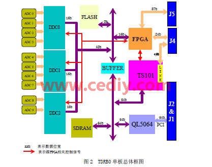
Modern digital receiving systems also require certain pre-processing functions to ease the pressure of subsequent data transmission and processing. TDRB0 uses DSP as the data processing unit and DSP+FPGA as the data transmission unit, which has strong computing power and IO interconnection capability. Considering that radar systems usually require large dynamic range and high precision, most of the current radar system digital signal processing modules use floating-point DSP devices and the super floating-point computing power of Analog Devices' TigerSHARC series DSPs. With IO interconnect capabilities, we chose TS101 as the hub for processing, storage, and data transfer for TDRB0.
TDRB0 has many external interfaces, which are distributed on the front panel and J1~J5. There are three paths for subsequent transmission of TDRB0 data: 1 PCI bus. Based on the CPCI bus, TDRB0 realizes 66Mhz and 64bit PCI interfaces by using the semi-custom chip QL5064. 2TS101's own four-way LINK port communicates with the TS LINK port of other boards through J4 and secondary backplane, and its transmission rate can reach 150MB/s; 3FPGA connects 81 bit IO pins on J4 and J5, which can be customized. It can also be used for the FPDP bus with a maximum transfer rate of 320MB/s.
2.2 Digital receiver platform construction In the rice band DBF system radar, a digital receiver consisting of multiple TDRB0 shares a 21-slot standard 6U CPCI chassis with a signal processor consisting of multiple signal processing boards. If the PCI channel of TDRB0 is used to transmit data to the signal processor, the customized secondary backplane can be omitted, but in this system, the required transmission data rate is high, and the shared PCI bus is difficult to bear such load. The LINK using DSP passes through the secondary backplane to form a set of dedicated LINK bus, which can guarantee the transmission bandwidth and is more flexible and convenient to implement. At the same time, through the secondary backplane, TDRB0 receives the timing signal sent by the timing board and the radar command word (as shown in Figure 3). 
In order to analyze the actual echo data of the radar offline, the digital receiver also includes a SCSI disk array, which can store the digital received signals of each channel in real time. Through a set of SCSI adapter boards, data flows from TDRB0 through the secondary backplane to the disk array. There are two sets of dedicated LINK buses in the digital receiver. One set connects multiple TDRB0 and signal processor, the data is transmitted to the signal processor to complete the normal radar signal processing, and the other connects multiple TDRB0 and SCSI adapter boards. Data is sent to the disk array storage through the transfer board. The two sets of buses do not affect each other, so they can work simultaneously or separately.
Prior to the joint adjustment of the entire radar system, an internal timing board provides the digital receiver with the timing timing required for debugging. When the whole machine is connected, the other subsystems of the entire radar system - waveform generation, receiving front end, etc. also need timing timing (as shown in Figure 1). At this time, it is more powerful to provide timing timing for the entire radar system. The interface is more abundant external timing board. In order to make the two sets of timing sequences not conflict with each other, a set of Mux is used on the secondary backplane, and the internal and external timings are gated according to the command of the upper computer, thereby determining whether the timing timing of the entire system is generated by the internal timing board or the external timing board ( image 3).
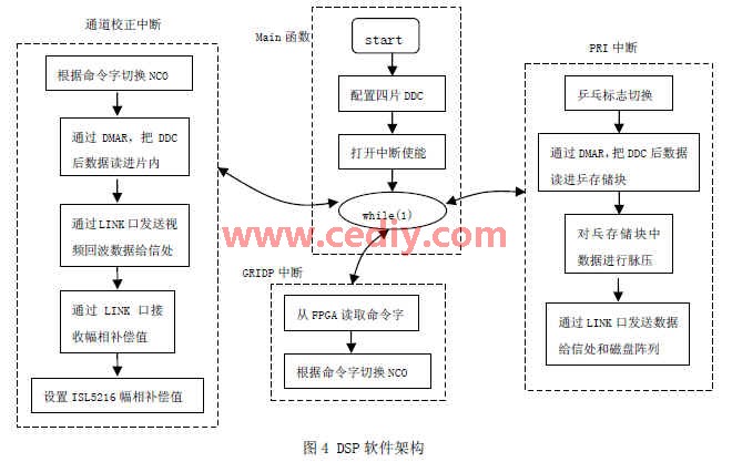
2.3 Implementation of Digital Receiver Software The DSP of TDRB0 not only completes the configuration of three DDCs, but also buffers and rearranges the data after 10 channels of ISL5216, and also completes the pulse pressure operation in radar signal processing, and passes the data after pulse pressure. The LINK port is passed to the signal processor. Since the digital receiver is closely related to the timing timing of the radar system, the software architecture of the DSP uses interrupt driving rather than data stream driving, as shown in Figure 4. After optimization, using DSP to complete the pulse pressure processing of one channel (1024-point frequency domain pulse pressure plus 512-point frequency domain pulse pressure) requires a total of 750μs. For a meter-band radar, the PRI is usually about several ms, then at a PRI time. Inside, there is enough time to complete the pulse processing of 10 channels.
In the DBF system radar, the inconsistent amplitude between the channels will cause the side lobes of the antenna pattern to rise [2], and the signal-to-noise ratio is reduced, which seriously affects the spatial filtering effect. Multi-channel amplitude and phase correction is achieved by multiplying the echo data by a correction factor when the amplitude and phase error between the channels is known. Since the number of radar channels is large, the correction factor is directly set in the ISL5216 for amplitude and phase correction, which can greatly reduce the computational load compared with the multi-channel amplitude and phase correction in the signal processor. Therefore, in the channel correction interrupt, each block of TDRB0 needs to obtain a correction factor from the signal processor, as shown in FIG.
The digital receiver uses the host computer to load the DSP program to the TDRB0 through the PCI bus. Due to the sharing of the PCI bus, the DSP program does not start to work synchronously. In order to ensure that the data between the boards is always synchronized, the timing timing is required to be provided after all the DSP programs of the board are loaded, so that all the DSPs of the TDRB0 enter the PRI interrupt at the same time, thereby ensuring the synchronization of the data between the boards. This sequence is achieved by controlling the timing of the Mux module on the secondary backplane to shield and gate the external timing module.
3 Conclusions The author of this paper is innovative: 1. Combining the development of a certain type of rice band DBF radar, a digital receiving board based on CPCI bus is proposed, which has the characteristics of high integration, strong modularity and large dynamic range. It has also proved to be of good reliability by long-term inspection in the field. Each channel operating in the radar system has been tested repeatedly: when the input signal is above 200Mhz in the 300khz bandwidth, the ENOB reaches 10.9bit, the dynamic range is typically 88dB, and the DDC filter has an out-of-band rejection of 70dB or more. The in-band ripple is less than 0.03dB. 2. With multiple TDRB0 as the core, supplemented by customized secondary backplane, internal and external timing module, timing switching module, SCSI data acquisition chassis and other debugging equipment, it constitutes a digital receiver for engineering application, which is convenient for external field joint debugging. Speed ​​up the progress of the project. Practice has proved that the digital receiver meets the project requirements and achieves the intended purpose.
Indoor High Resolution LED Curtain
Led Curtain/Led Mesh, Outdoor Led Display,Indoor Led Display,Light Box
Rental LED Display,Fixed LED Display Co., Ltd. , http://www.nbleddisplay.com