Abstract: Aiming at the shortcomings of the existing LED drive circuit with the electrolytic capacitor to limit the life, a design method of the LED drive circuit without electrolytic capacitor is proposed. This method uses Panasonic Panasonic MIP553 built-in PFC dimmable LED driver circuit chip, combined with external non-isolated bottom chopper circuit as the basic circuit structure, output stable current to meet the needs of LED work. At the same time, a protection circuit is designed to protect the load. The experimental results show that the controller chip can work stably, and can achieve a constant voltage output of 27V and a constant current output of 350mA.
LED (Light Emitting Diode) has become a new generation of green lighting source with its many advantages such as energy saving, environmental protection, high brightness and long life. As the LED lighting technology matures, it will eventually be used in all aspects of life and become a new favorite of lighting sources. However, high-efficiency, low-cost, high power factor and long-life driving power supply is the key to the luminous quality and overall performance of LED lamps.
The LED lamps on the market that replace ordinary bulbs are about 40 times longer than incandescent bulbs, which is equivalent to 40,000 hours. Because LED is a DC current driving part, the electric energy directly converted into light energy by the current flowing through, so it is also called photoelectric converter. Because there is no friction or mechanical loss, it is more efficient than general light sources in terms of energy saving. However, when the AC power is turned on, it is generally a DC stabilized power supply that uses rectifier parts and a smoothing circuit. The necessary electrolytic capacitor in this smoothing circuit will rise by 10 ° C due to the surrounding temperature and its own heat, resulting in a half life Therefore, electrolytic capacitors hinder the life of LED lighting fixtures.
In order to improve the life of the driving power supply, simplify the circuit, reduce the cost and increase the power density, it is necessary to remove the electrolytic capacitor. For this purpose, a high-brightness LED driving power supply without electrolytic capacitor is proposed.
1 Basic working principle of LED power supply
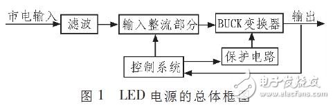
Adopt BUCK converter and IPD control to realize switching power supply, output constant current and voltage, and drive LED lamp. The overall block diagram of the circuit is shown in Figure 1.
In the main circuit part, a filter is connected immediately after the commercial power. Its function is to filter out the higher harmonics in the power supply and the surge in the power supply, so that the control circuit is less disturbed by the power supply. The input rectification part adopts an integrated rectifier bridge. The unidirectional conduction characteristic of the diode converts the alternating current floating at the zero point into unidirectional pulsating direct current, and then outputs the direct voltage under the action of the filter capacitor and the inductance. After the adjustment and control of MIP553 and BUCK circuit, the voltage for LED is output.
2 The specific design of the LED power supply
2.1 Design of input circuit
In order to extend the service life of the LED drive power and match it with the LED, the electrolytic capacitor in the circuit must be removed.
The design indexes of the circuit are: input AC voltage Vm: 198-264VAC / 50Hz; output voltage Vo: 27VDC; output current Io: 0.35A.
The input circuit includes a noise filter device, a safety insurance device, and an input rectifier device, as shown in Figure 2.
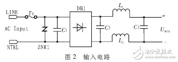
The noise filtering device is mainly composed of capacitors C1 / C2 / C3 and inductor L1. Its function is to reduce electromagnetic interference (EMI) in the frequency band less than 1MHz. This device can also be linked after AC and before the rectifier, the filtering effect is the same. The safety fuse is composed of a fuse and ZNR1. The fuse mainly prevents the circuit from being quickly cut off to protect the load when the peak current of the hazardous circuit is generated; ZNR1 is a surge absorber, which absorbs static electricity and surges from the input terminal to protect The circuit behind. The input rectifier device converts alternating current into direct current. The choice of input rectifier bridge: The voltage stress of the rectifier bridge diode is:

Considering the margin, choose TSC GBL205 (VR = 600V, IFAN = 1A).
2.2 Design of output circuit
The output circuit consists of a basic BUCK circuit and a Zener diode DD1. As shown in Figure 3.
2.2.1 BUCK converter and its advantages
Buck converter, also known as buck converter, series switching regulator, three-terminal switching buck regulator, is a single-tube non-isolated DC / DC converter with an output voltage equal to or less than the input voltage.

The input current is in operation is, when the switch is closed, is》 0; when the switch is open, is = 0, so is is pulsating, but the output current io is continuous and stable under the action of inductance, diode and capacitor of. Especially suitable for providing working current for LED.
Selection criteria for FRD1: rated current is greater than 2 times the output current, rated voltage is greater than the input voltage, and its reverse recovery time should also be within 100ns, considering the margin, the parameters of FRD1 are: 15A, 600V, trr = 50ns. Use similar The method chooses T1 and Cout, then their parameters are: T1: 680μH; Cout: 1μF, 50V.
2.2.2 Zener diode DD1
Within a certain range of low input voltage, if there is no such reverse device as DD1, there will be a reverse current flowing through the IPD at the moment the switch is turned off, and this current is not allowed in the IPD because of this This reverse current will cause damage to the IPD.
The stresses suffered by DD1: IDD》 2 · Io = 2 & TImes; 0.35 = 0.7A, UDD》 Uo, reverse recovery time trr 《100ns. Considering the margin, the selected parameters are: 3A / 60V / 75ns.
A 6 layer PCB board is in general a 4 layer PCB Board with 2 extra signal layers added between the planes. The 6-layer PCB classic stackup includes 4 routing layers (2 outer layers + 2 internal layers) and 2 internal planes (one for ground and the other for power). This enhances the EMI dramatically by offering 2 buried layers for high-speed signals and 2 surface layers for routing low speed signals. The signal layers should be closed to the adjacent planes.
6 layer PCB
Storm Circuit Technology Ltd , https://www.stormpcb.com