The 28 Gbps backplane feature of Xilinx UltraScale devices allows the network to operate at 1 Tbps.
Two years ago, IEEE's story pointed out that based on current trends, the communication network in 2015, the need to support capacity requirements 1Tbps, by the year 2020 needs to support 10 Tbps transmission capacity. According to the 2012 report, there will be nearly 15 billion fixed-line and mobile network devices next year, including interconnections between machines. For optical transport network (OTN) applications, the core node's bandwidth per wavelength is expected to reach 100G to 400G by 2015 and will increase to nearly 400G to 1T by 2020.
The Xilinx Virtex® UltraScaleTM All Programmable FPGA is an extension of the high-end FPGA family that supports the implementation of 1Tbps systems. With unprecedented performance, system integration and bandwidth, the Virtex UltraScale Series is ideal for a wide range of applications, including wireline communications, test and measurement, aerospace and military, and data centers.
Many companies have expressed the need for 1Tb network applications. These applications require transceivers to directly drive 25G/28G backplanes to address issues such as routing, crosstalk, differential insertion loss, and impedance matching. The Virtex UltraScale device solves these challenges perfectly, supporting 25G/28G backplane operation without a retimer, enabling support for 1Tbps applications.
Using an external retimer can create reliability issues and also requires a lot of very expensive PCB board space.
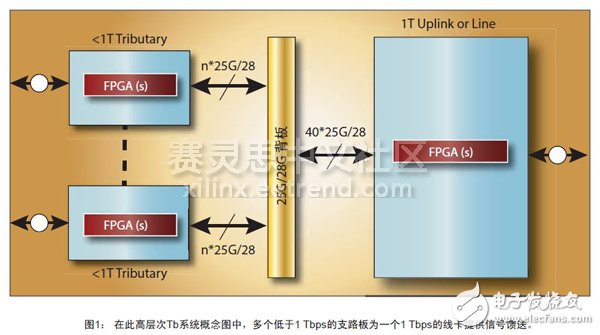
Example 1-Tbps designFigure 1 is a high-level block diagram of a possible general-purpose 1Tbps system. As can be seen from the figure, multiple tributary boards with less than 1Tb bandwidth (two in this figure) are connected to a 1T line card through a backplane running at 25G/28G.
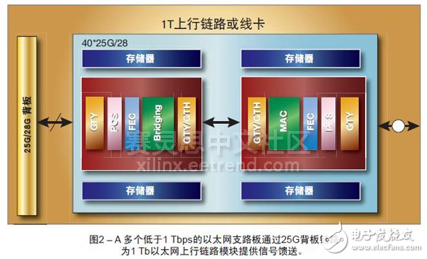
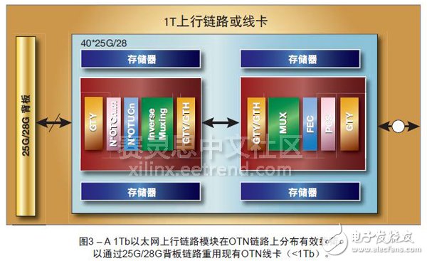
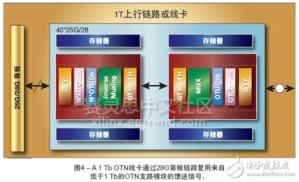
2, 3 and 4 are three possible more detailed block diagram 1Tbps Ethernet and OTN applications, all of which are based in Virtex UltraScaleFPGA build. 33 GbpsGTY transceiver may be connected to the CFP2 / 4 LR4 optical module and 25G / 28G backplane. According to the illustration, the 16 Gbps GTH transceiver is connected to the high speed memory.
These 1T applications must rely on backplane transceivers that support 25G/28G. Backplanes with 10G links face issues such as routing, crosstalk, differential insertion loss, and impedance matching.
These 1T applications must rely on an FPGA that can run directly on the backplane at 25G/28G. Using an external retimer can create reliability issues while also taking up a lot of very expensive PCB board space. The backplane retimer is an add-on and must be deployed on the line card and the tributary board. The voltage regulation module, distribution network, DC blocking cap, and reference clock required for the operation of the backplane retimer take up the board space of these PCBs.
Routable problemIn these examples, we show 40 channels running on the backplane at 25G/28G with a total bandwidth of 40 x 25 Gbps = 1 Tbps. The backsheet thickness is typically about 0.25 inches, depending on two factors: the mechanical requirements of the press-fit TIng, and the need for multiple channel routing support. If the backplane interface only supports 10 Gbps operation, the number of channels needs to be increased by 2.5 times. For each 1Tbps line card and tributary board, this will increase the number of backplane channels from 40 to 100. If the system requires 25 tributary boards and line cards, the total number of channels required will eventually be 100 x 25 = 2,500. This poses a big challenge to routing.
Using a backplane dielectric material such as Panasonic's Megtron-6 with a dielectric constant of approximately 3.65 and a standard conductor width of 7 mils, we found that the stack height of each differential strip pair is: 16 odd-mode impedance per 100 Ω. Mill.
Assuming a typical backplane connector spacing of 2 mm, one channel can be deployed between the connector pins of each layer. Therefore, each layer of the backplane can support 10 channels per channel (send + receive) per layer. For 25 Gbps, typically 16 wiring layers are required with a total board thickness of 16 mils x 16 wiring layers = 0.256 inches. For 10 Gbps, the thickness is 0.640 inches (16 x 2.5 = 40 wiring layers, total plate thickness is 16 mils x 40 layers = 0.640 inches). However, the maximum thickness of the backing plate is usually determined by the depth-to-width ratio of the via holes. Typical via holes are 15 mils in diameter and have a standard depth to width ratio of 25:1. This means that the upper thickness of the backing plate is approximately 14 x 25 = 350 mils. Therefore, the 10G backplane cannot support 1T applications.
Crosstalk problemFor 1T applications, another key advantage of the 25G backplane versus the 10G backplane is crosstalk. Crosstalk is usually caused by channel distance. The more backplane channels, the higher the chance of crosstalk. Therefore, a backplane with 1000 25G channels has a lower probability of crosstalk than a backplane with 2500 10G channels.
However, most dielectric materials are not completely homogeneous and therefore have a far-end crosstalk (FEXT) effect. In addition, crosstalk occurring in the via hole area around the backplane connector is typically far-end crosstalk.
Since crosstalk in the backplane system has both near-end crosstalk (NEXT) and far-end crosstalk (FEXT) effects, designers must be careful to reduce the crosstalk noise component associated with the total noise budget. There is a mutual capacitance Cm (electric field) between the sensitive device and the interference source network, and there is a mutual inductance Lm (magnetic field). The mutual inductance induces a current (Lenz's law) on the sensitive device line opposite the interference source network. Mutual capacitance transfers bidirectional current across the sensitive device line through mutual capacitance. The currents on the near-end and far-end sensitive device lines together produce NEXT and FEXT effects.
I(Next) = I(Cm) + I(Lm) while I(Fext)= I(Cm) – I(Lm).
NEXT is always positive. FEXT can be positive or negative.
Differential insertion lossThe insertion loss of the channel is an important parameter when establishing a reliable link. IL depends on two factors: connector loss and dielectric loss. When using a dielectric material such as Panasonic Megatron-6, the tangential loss is 0.004. Figure 5 shows the insertion loss for a 1 meter long trace. The surface roughness is 1 micron (ultra-low profile). Since the maximum thickness of the backing plate is 0.350 inches, trace width of the back plate 10G has dropped to only 3 mils wide, to allow the wiring layer 40 laid on the back sheet 0.350 inches thick, while the odd mode impedance of the differential maintained at 100Ω . For the 25G backplane, the trace width is 7 mils and 16 layers of wiring can be laid on a backplane with a maximum thickness of 0.350 inches.
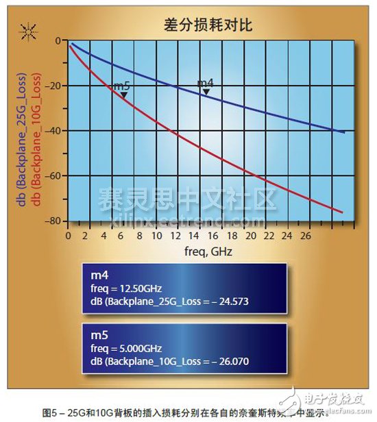
Figure 5 shows that the differential insertion loss of the 10G backplane is higher than the 25G backplane. This is because the 10G backplane increases the number of routing layers within the maximum backplane width, resulting in a narrower trace width.
We have already pointed out that Virtex UltraScale devices support 25G/28G backplane operation without retimer to support 1Tbps applications. These future 1Tbps applications require receivers to directly drive 25G/28G backplanes to address routing, crosstalk, differential insertion loss and impedance matching issues. Excessive number of wiring layers, larger connectors, and manufacturing reliability issues associated with via hole depth-to-width ratios can have an impact.
It is used for continuous level measurement. The signal transmitted by its sensor is collected by the receiving system after being reflected by the target, and the distance of the target is determined by measuring the reflection running time. Then the level distance is converted into an output signal and output as a measured value.
The liquid level radar is applicable to the continuous non-contact liquid level measurement of liquid cargo tanks and overflow tanks of oil tankers and chemical carriers. It is also applicable to the liquid level monitoring of other oil tanks, towers, tank equipment and oil production platforms. Its measurement results are not affected by medium replacement, temperature change and gas or steam coverage.
Radar Level Gauge Sensor,Level Gauge Sensor,Level Sensor Durable,Durable Radar Level Gauge Sensor
Taizhou Jiabo Instrument Technology Co., Ltd. , https://www.taizhoujbcbyq.com