From the perspective of the inventor to see the invention and use of the triode
I am still that point of view, we must stand inventor's point of view to see the problem, only in this way, all problems can be solved. Because the content of the mold is the invention - the use of - to find problems - to improve - re-invention - the process of reuse, is what we learn invented and used by predecessors.
We use diodes and triodes as an example. The diode controls the flow of electrons in the wire, and the transistor controls how much electrons flow in the wire. This is also the root of "electronic technology." Theory makes it easy to experiment.
In the following, the transistor is used as an example to illustrate the control of the current in the wire. To control the current in a wire, the wire must first be disconnected. The two ends of the break are called the C and E terminals respectively (C and E is actually an output loop. If we add a device between C and E, this device can make the current flow in from the C terminal and can flow out from the E terminal. At the same time, this current can be controlled by us, so this The device is successful.
In order to achieve the above requirements, next we put an NPN (or PNP) structure semiconductor between CEs. However, the problem is that in this case no matter how to add power between C and E (do not break through In the case of CE), there will be no current in this conductor of CE. We also know that the direction of the flow of electrons is opposite to the direction in which people define the current (since it was thought that current flowed through the wires was current), so we took the middle semiconductor out of an electrode (B-pole) between BEs ( Actually, it is applied to the emitter junction (see PN junction characteristics). Adding a forward voltage, the emitter emits electrons to the base region to form an E-source current. However, to realize this current is from the C terminal. In and out of the E terminal, the electrons emitted by the emitter must be collected at the C terminal. In this way, we need to apply a positive voltage between C and E so that the collector junction is in the reverse breakdown state. The electrons can be collected to the C pole. This ability to collect electrons is stronger than the ability to emit electrons. It is like a big pocket. How much I emit in your launch area (so that you can understand the output characteristics of the triode, when B When the polarity of the current is constant, as the CE voltage increases, the current of the C-pole will no longer increase. Because the current of the B-pole is constant, the amount of electrons emitted by the emission region will be definite, and your collection ability will not be excessive. Electronics) In this way, the device is made to allow the current to flow from the C terminal to the E terminal (because I originally assumed that they were between the ends of the wire that was disconnected by me). The most ideal current is to flow into the C terminal. Equivalent to the current flowing out of the E terminal. At the same time, this current is controlled by a BE voltage (or signal). However, the transistor is not an ideal device because the C terminal current is not equal to the E terminal current. A part of the current flows through the B terminal. We try our best. The current at the C-terminal is equal to the current at the E-terminal. Therefore, this is the fundamental reason why the concentration of the base region should be low and thin at the process, and the area of ​​the collector junction must be large.
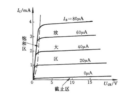
Talk about Ic controlled by Ib:From the foregoing description, we already know that the emitter current Ie is controlled by the emitter junction voltage. Since we have taken technical measures, the collector current Ic is approximately equal to the emitter current Ie, so that it can be said that the collector current Ic is affected by the emitter junction. Voltage control. We can also see from the triode input characteristic curve that when the relationship between Vbe and Ib is at the approximate straight line of the characteristic curve, the base current Ib is linear with the emitter junction voltage. Thus, it can be said that the collector current Ic and the base current Ib is proportional. Often we will stand at a different point of view. From the point of view of current amplification, we just said that the collector current Ic is much greater than the base current Ib, and they are proportional. Therefore, when the calculation is performed, It is said that the collector current Ic is controlled by the base current Ib. This is actually the point of view of people standing differently (from the current amplification point of view), in fact, the collector current Ic is still controlled by the emission junction voltage, wait until the high-frequency small-signal model, it will say that the collector current It is controlled by the launch junction voltage.
The role of Uce voltage is to collect electrons, its size can not determine the size of Ic, can be seen from the triode output characteristics curve, when Ib is certain (that is, Ube is certain), even if Uce increases, Ic will not change, but The curve is somewhat upturned. In fact, this is a problem with semiconductor materials. In fact, Ie is controlled by the emitter junction voltage seen from the input terminal (see the triode high-frequency small-signal model). When the Uce voltage is applied, the emitter junction is already turned on, and its effect is not at the emitter junction but at the set level. Electric junction, Uce voltage is added in order to make Ic is basically equal to Ie, so Ic is controlled by the emission junction voltage, people convert this control into Ib control for calculation convenience, because it is said that it makes people less understand the transistor. The principle of work.
From the perspective of the output loop controlled by the input loop signal, Ic is not controlled by Ie. However, Ic is actually caused by Ie. Therefore, it can be said that Ic is affected by Ie, which is also influenced by the transistor manufacturing process. If you take two back-to-back diodes, you can't do anything.
Although the transistor is not an ideal device, its invention is already of epoch-making significance. Because it has a small amount of current at its B pole, because the existence of this current means that the input circuit has energy. If I can control the current of your output circuit without using energy, then this is cheap, so later people invented it. FET. In fact, the idea of ​​inventing the field effect transistor is also the same as that of a triode. It is to use a voltage to control the current in the wire, but this time the input loop is hardly energy-consuming. At the same time, the currents at both ends of the device are equal.
Take a look at the triode application from the perspective of the user (non-designer):
The two basic applications of a transistor are "controllable switching" and "linear amplification of the signal."
Controllable switch: between C and E is equivalent to a controllable switch (of course. This switch has a certain parameter requirements), when there is no voltage between BE, CE cut-off (between CE is disconnected); and when BE The voltage increases greatly, the number of electrons emitted by the emitter is large, and the currents at the C and E poles are large. If there is a load in the output loop (note that the output loop will not saturate between loads CE) Since most of the power supply voltage of the output loop is applied to the load, the voltage between the CEs will be very small, the CEs will be in a saturated state, and the CEs will be short-circuited. In the saturation case, although the C-pole current is larger than the base current, the C-pole current and the input loop current (base current) do not have a proportional relationship of β.
Taking the simplest circuit as an example, we have a flashlight in our home. The flashlight has three elements (general meaning): power supply, light bulb (load) and switch. The switch here needs to be manually closed and disconnected. The triode is used instead. Switch we can achieve signal control, the computer can control the circuit at the far end. Control high voltage, high current, please also look at the IGBT and other power chips and modules, it is really shocking.
Saturation on the other hand: As can be seen from the output characteristic curve, when IB is constant, the VCE voltage does not have to be large, and the output characteristic curve is flattened. This means that the voltage VCE for collecting electrons does not have to be very large. It is actually less than 1V. That's right, but, in fact, we are adding a large voltage power supply to the output loop. You no longer need to increase VCE. We see that IB has no effect on the size of the IC after IB is increased (ideally). So if you want to collect the electrons that you launched, VCE doesn't use a lot of voltage at all.
However, under normal circumstances, we will add a load in the output loop. When the voltage across the load is less than the power supply voltage, other parts of the power supply voltage are added to both ends of the CE. At this time, the triode is in a linearly amplified state. However, when the theoretical value of the voltage across the load is greater than the supply voltage, the triode is in a saturated state, and ICs in this case need not be very large.
So don't think VCE must have a very large triode collector to collect electrons. You can see that the voltage of collecting electrons is very small. For the saturation problem, in addition to the saturation caused by the current mentioned in the previous paragraph, we can also consider the voltage from the perspective of the triode. The power supply voltage is 12V and the base current is 40μA. The collector current is 2mA. If the collector is connected to a 3K ohm resistor, VCE=6V. When this resistance is changed to 30KΩ, VCE tends to zero. In this case, the triode is also saturated, so from the voltage point of view, the collector current is not necessarily very large, in the case of selecting the appropriate load resistance, the triode can also be saturated, so the saturation is related to the load, if The voltage of the power supply is very high. VCE is certainly insignificant when it is saturated with such a little voltage. Therefore, it is equal to about zero in many places, but it cannot be said that it has no electronic collection capability.
Linear amplification of the signal: In this case, the linear relationship between the C-pole current and the B-pole current is IC=βIB (the voltage between the BE is greater than the dead-zone voltage, and at the same time, the VCE does not tend to zero), and the C-pole current ratio The B-pole current is much larger. It is known in the past that the magnitude of the C-pole current is controlled by the BE voltage (people are convenient to analyze the problem, and this control relationship is said to be that the C-pole current is controlled by the B-pole current). In fact, the car running around on the road is an amplifier. It magnifies the signal from the driver. It is also a linear amplification, which is the amplification of energy. The extra energy comes from the burning of gasoline.
Most of the content of this module from the triode small signal model starts with the small signal amplification problem. The four circuits of the common emitter, the common collector, and the common base are the basic ones. The others are the combination of them. Their circuit composition, circuit AC/DC analysis, and circuit performance analysis are key.
The other issues are power amplification, the design of analog integrated operational amplifier internal structures, the application of operational amplifiers, how to reduce nonlinear distortion and amplification stability (negative feedback), and sine wave generation (positive feedback).
Modular electricity is grasped from the details and overall.
Modular learning:
From the user’s point of view, in fact, this course is not difficult. Students are often confused by secondary issues such as “low births, many children, drifts, and proliferation†mentioned in the book. They do not grasp the main issues. The problem is caused by defects in the semiconductor material itself. People have come up with various solutions to overcome these defects. Therefore, many of them are skills and ideas that people come up with. From the point of view of the three electrodes of the triode connected to the metal, only the directional flow of the free electrons in the metal will have the current, and what kind of hole in the metal or the like will hold the line of sight of the people in the interior of the triode. It must be difficult for people to understand. If you jump out to see the problem, you will understand why the scientist invented it at the time and it will make you suddenly see. However, from the designer's point of view, there are many problems that need to be considered. Otherwise, the device performance you design will not be as good as others' design. Of course, there will be no market. If anyone can find a material whose performance is better than that of semiconductors, he will certainly be admired by the world. Therefore, when learning to model electricity, we must use engineering thinking to consider the problem. For example, why invent it? What is its use? What problem can it solve? What are the shortcomings? How do people improve? and many more.
Let's talk about controllable switches:
The transistor must work in saturation or cut-off state. At this time, C and E are equivalent to controllable switches, and B is added with input signals. In order to prevent the damage of the transistor, the B-pole must be connected to the current limiting resistor. The remaining problem is that the controlled load Should it be connected to C pole or E pole? How big is it? How much drive voltage? How big is the current? Can the triode you choose be competent? What should I do if I'm not qualified? What device to use? How to isolate low pressure and high pressure? and many more.
Talk about the linear amplification of the signal:
In this case, the C-pole current is β times the B-pole current. Take the triode amplifier circuit as an example:
(1) DC operating point, why should there be a DC operating point? What causes the instability of the work site? What measures are taken to stabilize the DC operating point?
Why DC operating point? It is because the PN junction only has a current (silicon material) passing through it when it is applied with a voltage of 0.5 V or more, and the amplitude of the weak alternating signal that we want to amplify is very small. This signal is directly added between the base and the emitter of the transistor. The base is without current, of course, the collector can not have current. Therefore, after we add DC to the base, we use the NPN tube as an example. The DC of the three circuits of cascode, cascode, and common collector is a direction. Regardless of the type of transistor circuit, their DC current direction is the same. After the input (transmitting junction) joins the weak AC small signal, these output loop currents can only be perturbed, and the direction of these currents cannot be changed as a whole. However, this output loop current has a disturbance signal that is affected by the input AC signal. What we need is this disturbance signal (output AC signal). This disturbance signal is larger than the input signal. This is the amplification, and it can be said that the amplification is actually The output loop current is controlled by the input signal.
If the DC operating point is set properly, that disturbance signal is proportional to the input AC small signal, and larger than the input signal, what we want is this effect.
(2) What are the advantages, disadvantages, and disadvantages of common-emitter, common-collector, and common-base circuits? How to overcome the nonlinearity of the circuit? Why Common-to-Communist Circuits Can Extend the Frequency Band? Why is the common-collector amplifier circuit placed on the final stage of a multi-stage amplifier circuit? What are the requirements for the input stage of a multi-stage amplifier circuit? What is the purpose of designing a current source in an integrated circuit? What is its role? How to overcome zero drift caused by direct coupling? Why design deep negative feedback? What are its advantages and problems? What is the reason for deep negative feedback self-excitation? What is the structural phase shift of the circuit? What is the additional phase shift of the circuit? Under what circumstances is there an additional phase shift between the output signal of the circuit and the input signal? and many more.
(3) Integrated operational amplifiers, in order to overcome the nonlinearity of semiconductor devices (different amplitude signals have different magnifications), people intentionally made high-gain integrated operational amplifiers. The external two resistors constitute the in-phase or reverse ratio. Amplifier circuit, when the voltage magnification of the entire circuit is approximately independent of the semiconductor characteristics (deep negative feedback conditions), the amplification factor is only related to the external two resistors, and the temperature characteristics of the resistive material is better than the semiconductor material, while linear The characteristics have also improved. When calculating, pay attention to the use of "virtual shortness" and "virtual power-off". It is too simple to learn here. Therefore, if you do not consider the cost, who will use the amplifier circuit composed of discrete components, you must adjust DC operating point. There are many other applications of integrated operational amplifiers, such as active filters, signal generation circuits, and so on.
The difference between negative feedback self-oscillation and sine wave generation circuitNegative-feedback self-oscillation is caused by an additional 180-degree additional phase shift in the feedback loop due to an unknown frequency signal. The negative-feedback circuit becomes positive feedback for this frequency signal, and at the same time, the frequency signal The loop gain is again greater than one. In this case, the negative feedback circuit is self-excited (for other frequency signals, this circuit is also negative feedback). The sine wave oscillation circuit is a positive feedback that people intentionally introduce. It can be said that the countless frequency signals are positive feedback. In this case, there is no need for additional phase shift in the loop. However, there are too many such signals, so people A frequency selective circuit needs to be designed in the feedback loop to select a certain frequency signal. Of course, this selected frequency circuit does not require extra phase shift for the selected signal.
Panasonic provides extremely dependable electronics assembly equipment in the areas of SMT (surface mount technology), PTH (pin through-hole), and processes involving microelectronics back-end packaging of any-mix circuit manufacturing. We offer first-class equipment ranging from screen printers and dispensing, through component placement and inspection, up to axial and radial insertion, die bonding, die attach and flip chip. Our equipment is used all around the world to enable the production of the most modern technology.
Our variable machines in modular format support a large range of technologies and, from the installation of just one machine through to assemblies of over 1,000, can take care of processes such as, COB (chip on board), SOP (system on package), epoxy die attach, POP (package on package), 3D packaging, TS (thermo-sonic) and TC (thermo-compression) processing, plasma RIE surface cleaning, plasma ICP etching, and thin wafer plasma dicing. To perform odd-form placement and end-of-line work, we also offer automated equipment.
Panasonic Smt Machine,Panasonic Chip Mounter,Smt Panasonic Machines,Panasonic Smt Equipment
Shenzhen Keith Electronic Equipment Co., Ltd. , https://www.aismtks.com