Power supply noise is a type of electromagnetic interference, and its conducted noise spectrum is approximately 10 kHz to 30 MHz, up to 150 MHz. Power supply noise, especially transient noise interference, has a fast rising speed, short duration, high voltage amplitude, and high randomness, which is likely to cause serious interference to microcomputers and digital circuits.
Application of oscilloscope frequency domain analysis in power supply debugging
This article talks about the power supply noise measurement problem that has been the most concerned for so many years. It has the most practical experience summary, the test cases are supported by the test cases, and the simulation analysis is combined.
In the analysis of power supply noise, the more classical method is to use the oscilloscope to observe the power supply noise waveform and measure its amplitude, and then judge the source of power supply noise. However, as the voltage of digital devices is gradually reduced and the current is gradually increased, the design of the power supply is more difficult, and more effective testing methods are needed to evaluate the power supply noise. This paper is a case of using the frequency domain method to analyze the power supply noise. When observing the time domain waveform cannot locate the fault, the time-frequency conversion is performed by the FFT (Fast Fourier Transform) method, and the time domain power supply noise waveform is converted into the frequency domain for analysis. When debugging the circuit, the signal characteristics can be viewed from the two angles of the time domain and the frequency domain, which can effectively speed up the debugging process.
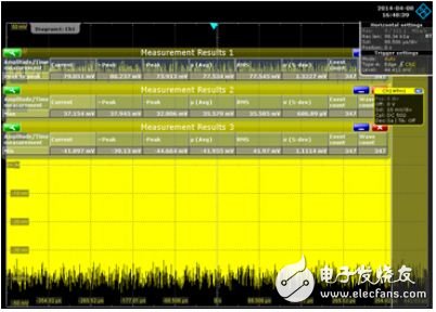
During the debugging process of the board, it was found that the power supply noise of a network reached 80mv, which exceeded the requirements of the device. In order to ensure stable operation of the device, the power supply noise must be reduced.
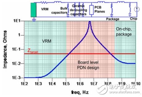
Review the principle of power supply noise rejection before debugging the fault. As shown in the figure below, the different frequency bands in the power distribution network are suppressed by different components. The decoupling components include the power supply adjustment module (VRM), decoupling capacitors, PCB power ground plane pairs, device packages, and chips. The VRM consists of a power chip and a peripheral output capacitor, which acts on the DC to the low frequency band (around 100K). The equivalent model is a two-element model consisting of a resistor and an inductor. Decoupling capacitors are preferably used with capacitors of multiple orders of magnitude to cover the mid-range (approximately 10K to 100M). Due to the presence of wiring inductance and package inductance, it is difficult to instantaneously build a large number of decoupling capacitors at higher frequencies. The PCB power ground plane pair forms a flat-panel capacitor that also has a decoupling effect, which is approximately tens of megabits. Chip packages and chips are responsible for high frequency bands (above 100M). Currently, high-end devices generally add decoupling capacitors to the package. At this time, the decoupling range on the PCB can be reduced to tens of megabits or even several megabytes. Therefore, in the case of constant current load, we only need to determine which frequency band the voltage noise appears in, then optimize the decoupling component corresponding to this frequency band. The two decoupling elements cooperate in the adjacent frequency bands of the two decoupling elements, so the decoupling elements of adjacent frequency bands are also taken into account when analyzing the critical point of the decoupling element.
According to the traditional power supply debugging experience, firstly, some decoupling capacitors are added to the network to increase the impedance margin of the power network, and the power network impedance in the middle frequency band can meet the requirements of the application scenario. As a result, the ripple is only reduced by a few mV, and the improvement is minimal. There are several possibilities for generating this result: 1. The noise is at a low frequency, and is not within the range in which these decoupling capacitors are active; 2. The increased capacitance affects the loop characteristics of the power regulator VRM, and the impedance reduction caused by the capacitor and the VRM The deterioration has been offset. With this question in mind, we consider using the oscilloscope's frequency domain analysis to look at the spectral characteristics of the power supply noise and locate the source of the problem.
The frequency domain analysis function of the oscilloscope is realized by Fourier transform. The essence of the Fourier transform is that any time domain sequence can be expressed as an infinite superposition of sine wave signals of different frequencies. We analyze the frequency, amplitude and phase information of these sine waves, which is the analysis method of switching the time domain signal to the frequency domain. The sequence sampled by the digital oscilloscope is a discrete sequence, so the most commonly used in our analysis is the Fast Fourier Transform (FFT). The FFT algorithm is optimized for the discrete Fourier transform (DFT) algorithm, and the amount of computation is reduced by several orders of magnitude, and the more points that need to be operated, the greater the computational savings.
There are several key points to note about the FFT transformation of the noise waveform captured by the oscilloscope.
1. According to the Nyquist sampling law, the spectral broadening after the transformation corresponds to 1/2 of the sampling rate of the original signal. If the sampling rate of the original signal is 1 GS/s, the spectral broadening after the FFT is at most 500 MHz. ;
2. The frequency resolution after the transformation (RBW ResoluTIon Bandwidth) corresponds to the reciprocal of the sampling time. If the sampling time is 10 mS, the corresponding frequency resolution is 100 Hz;
3. Spectrum leakage, that is, the spectral lines in the signal spectrum interfere with each other, and the spectral lines with lower energy are easily overwhelmed by the leakage of adjacent high-energy spectral lines. Avoid spectrum leakage. Synchronize the acquisition rate with the signal frequency as much as possible, extend the acquisition signal time and use the appropriate window function.
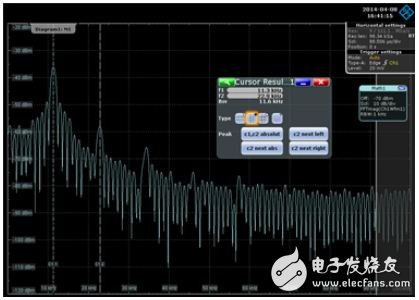
The power supply noise measurement does not require a high sampling rate, so a long time base can be set, which means that the acquired signal time can be long enough to be considered as covering the time span of the entire valid signal. function. Adjust the above settings to get a more accurate FFT transformation curve, and then use the zoom function to view the frequency points of interest. In the following figure, the main energy of the power supply noise is concentrated around 11.3 KHz, and the frequency is resonated at the fundamental frequency. According to this, it can be inferred that the impedance of the PDN network at 11.3 KHz cannot meet the requirements, and the impedance of the capacitor at the frequency point is also relatively high, so that the impedance cannot be reduced, so that increasing the capacitance in front does not reduce the power supply noise.
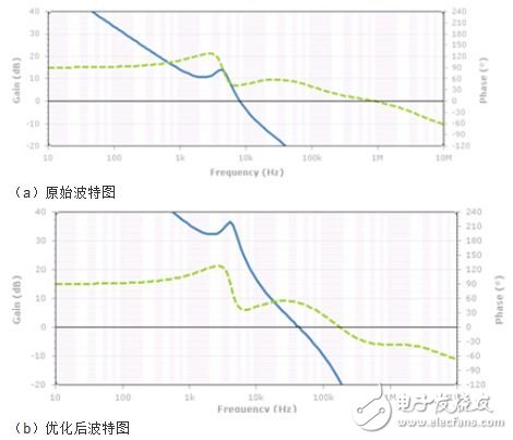
In general, 11.3KHz should be the jurisdiction of the VRM. The large noise here indicates that the VRM circuit design cannot meet the requirements. Here, the performance of VRM is analyzed. There are many methods for VRM analysis. Here, the method of simulating the loop diagram of the feedback loop is mainly used. The Bode diagram mainly observes several key information: 1. Crossing frequency, the frequency point of the gain curve crossing the 0dB line; 2. Phase margin, the phase value corresponding to the phase curve at the crossing frequency; 3. Gain margin, phase in- The gain value corresponding to 360°. Here we mainly focus on the two indicators of crossing frequency and phase margin. It can be seen from the loop Bode diagram of the VRM (as shown in the following figure a) that the VRM crossover frequency is around 8KHz and the phase margin is 37 degrees. There are two problems here: First, the phase margin of the VRM generally needs to be greater than 45 degrees to ensure the stable operation of the loop. Here, the phase margin is slightly smaller, and the phase margin needs to be increased. Secondly, the crossing frequency is too low, crossing the frequency near the VRM. The adjustment function is gradually reduced, and the bulk capacitor does not function at this frequency, so there is a high impedance near 8KHz, and the noise suppression effect of this frequency is poor. Figure (b) below shows the Bode plot after optimizing the VRM loop. The phase margin is adjusted to 50 degrees and the crossover frequency is pushed to about 46KHz.
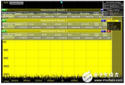
For the optimized VRM verification ripple, it can be seen that the ripple is significantly reduced to 33mv, which can meet the device requirements.
The above case is the process of quickly locating the power supply problem using the oscilloscope FFT function. From this example, we can see that the oscilloscope's frequency domain analysis function can play a big role in circuit debugging. The oscilloscope's FFT function combined with long memory depth makes it easy to analyze low-frequency long-period signals. This advantage is prominent in digital circuit debugging.
Tv Speaker,Wireless Soundbar,Single Soundbar Speaker,Soundbar With Wireless Subwoofer
Newmax Electronics Co.,LTD , https://www.fspeaker.com