Design and Implementation of Software Filtering Algorithm Based on FPGA
With the development of digital electronic technology, digital circuits have gradually evolved from early discrete components into integrated circuits, and the requirements for circuit design are getting higher and higher. Especially the emergence of programmable logic devices has made the design method of modern digital systems with hardware as the carrier and computer software as the development environment mature. The advantages of programmable logic device design flexibility, powerful functions, online modification, and high efficiency are favored by many electronic designers. At present, most field programmable logic array (FPGA) chips are voltage-sensitive chips. Based on the reconfigurable CMOS-SRAM cell structure, the data is volatile, works in a low voltage state, and is susceptible to interference, especially in industrial control and military applications. Occasionally, the external electromagnetic environment is bad, and the clutter pulse of circuit coupling and space radiation will affect the stability of FPGA operation.
Interference pulse and glitch signal are the main factors affecting the stable operation of the FPGA. In order to ensure that the input signal changes once, the circuit only makes a correct response, and the input signal must be filtered. To achieve signal filtering, hardware filtering and software filtering can be used. Compared with hardware filtering, software filtering does not require hardware circuit support, which can reduce the use of components and reduce costs. More importantly, software filtering is easier to modify. Therefore, software filtering is often used to achieve signal filtering in circuits. problem. The signal filtering function is realized by VHDL language programming. The delay filtering method and the decision filtering method are introduced. The reliability of the above two filtering methods is proved by experiments.
1 delay filter
The filtering principle of the delay filtering method is to identify the pulse width of the input signal, and effectively suppress the interference signals which are greatly different from the width of the real signal. The specific implementation process is that after detecting the change of the state of the input signal, the input signal delayed by a period of time T and the pulse width is less than the delay time T is considered as an interference signal, and is filtered out; the pulse width is greater than the delay time T The input signal is considered to be a real signal and is output. For different pulse width interference signals, the corresponding signal delay can be realized by setting different parameters, so as to achieve effective filtering.
1. 1 Determination of delay time T
The delay time T depends on the pulse width T' of the interference signal. The delay time T is too short (T<T'), the filtering is incomplete, and the interference signal with pulse width greater than T will still cause the circuit to malfunction; the delay time T is too long (T>>T'), which will cause resources. Waste, reducing the efficiency of the circuit.
Here, a certain type of twist switch input signal is taken as an example to describe how to determine the delay time. T. Because of the elastic action of the mechanical contact of the twist switch, when the switch is toggled, it is inevitable to close and close the contact. The moment of opening produces a series of jitters. In order to more accurately estimate the interference pulse width T' generated when the toggle switch is generated, the oscilloscope can be used to measure the switching signal multiple times. It is found that the jitter time of the twist switch signal does not exceed 1.5 ms. It is a switching signal waveform that has not been filtered.
In Figure 1, the abscissa represents time, each cell represents 50μs, the ordinate represents voltage, and each cell represents 1 V. It is obvious from the figure that there is a series of jitters before the switching signal reaches a steady state, and the jitter time is less than 1. 5 ms. Here, according to the actual situation, determine the delay time T = 2 ms.
1. 2 delay filter program design
The delay filter program is implemented by a counter. The modulo value N of the counter depends on the delay time T and the period TCLK of the sampling clock CLK. If the initial value of the counter is 0, then N = T /TCLK-1. Write a flowchart of the delay filter.
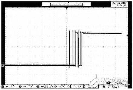
Figure 1 Unfiltered switching signal
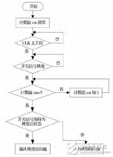
Figure 2 delay filter program flow chart
When it is detected that the state of the switch signal changes (here, from '0' to '1' as an example), the counter starts counting, and when the count value of the counter counts to N, if the switch signal remains in the state after the change '1', then output '1', otherwise, it is considered to be an interference pulse, which is filtered out.
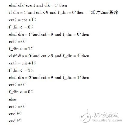
When the sampling clock frequency is 5 kHz, TCLK = 0.2 ms, to achieve a delay time of 2 ms, if the initial value of the counter is 0, then the counter modulus value N = 9. The specific VHDL language program process is as follows:

1. 3 delay filter program simulation
The switch signal din is set to the ideal signal and the jitter signal respectively, and the simulation is performed by using Quartus II8.0 software. FIG. 3 and FIG. 4 are the delay filter simulation waveform diagrams of the ideal signal and the jitter signal, respectively.
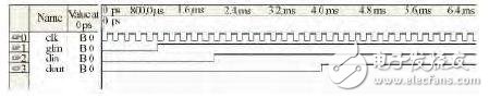
Figure 3 ideal switching signal delay filter simulation waveform
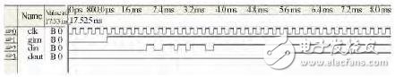
Figure 4 jitter switch signal delay filter simulation waveform
In the figure, clk is the sampling clock, glrn is the reset signal, din is the switch input signal, and dout is the delay filtered output signal. It can be seen from Fig. 3 that the time delay from the change of the switching signal to the change of the output is 2 ms. As can be seen from Fig. 4, the delay filtering program effectively eliminates the jitter interference of the twist switch, and verifies the Theoretical feasibility.
1. 4 delay filter program actual verification
In order to verify the actual filtering effect of this delay filter program, it is downloaded to Xilinx's Spartan3 series FPGA chip XC3S400, and the filtered switch signal is measured multiple times with an oscilloscope to obtain the output signal waveform shown in Fig. 5. In Figure 5, the abscissa represents time, each cell represents 10μs, the ordinate represents voltage, and each cell represents 1 V. As can be seen from Figure 5, the filtered switching signal no longer has jitter, the delay filter program The actual reliability is verified.
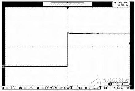
Figure 5 Delayed filtered output signal waveform
1. 5 delay filter program resource occupancy rate
In the design of electronic circuits, the resource occupancy of FPGAs is an important issue that we should consider. If the resource occupancy of the FPGA is too large, it will increase the burden on the FPGA and affect the running speed of the entire circuit. Table 1 shows the resource occupancy of the delay filter program in the XC3S400 chip.
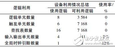
Table 1 Resource occupancy of the delay filter program
1. 6 characteristics of delay filtering
Delay filtering is more suitable for filtering the interference signal with known pulse width, so that the delay time can be determined more accurately. It is not because the delay time is too short, the filtering is not ideal, and the delay time is not too long. It leads to waste of resources. Moreover, the delay program can not only effectively eliminate the jitter of the switch type signal, but also filter out other spikes such as interference and noise, and has strong anti-interference and high reliability.
If there are multiple input signals in the circuit, the delay program is executed when the state of any one of the input signals is detected, and the change of other input states will not be detected during the execution of the delay program, so the identifiable action is detected. The interval cannot be less than the delay time T, especially when the state of the multiple input signals is concentrated in a short time, the performance of the circuit is seriously degraded. Moreover, due to frequent execution of the delay program, the efficiency and real-time performance of the system are affected.
Bifacial Solar Panel,Bifacial Solar Modules,Best Bifacial Solar Panels,Bifacial Solar Panels Price
Wuxi Sunket New Energy Technology Co.,Ltd , https://www.sunketsolar.com