As semiconductor technology continues to advance, it now allows for the integration of thousands of logic gates on a single chip, making system-on-chip (SoC) a dominant force in the future of integrated circuit (IC) development. However, when we refer to SoCs today, we are often talking about systems that combine digital baseband processing with data converters, high-speed analog I/Os, and even some RF circuits—provided they aren't too complex.
One of the major challenges in SoC design is the integration of RF circuits, largely due to process technology incompatibilities. Integrating RF components onto a digital die can reduce yield or increase testing costs, both of which significantly impact production expenses. This makes RF integration a tough hurdle for many designers.
But the challenge goes beyond just manufacturing. From an SoC system perspective, integrating RF components introduces complex design, implementation, and testing issues. These challenges span from circuit design to physical layout and final production, making the task more intricate than it appears at first glance.
Fortunately, new advancements in CMOS technology have started to change the game. With improved process nodes, RF integration is becoming more feasible. This allows developers to move RF signal processing into the digital domain, reducing the need for complex analog designs. Instead of dealing with analog components, engineers can now use familiar digital tools and processes to handle RF signals efficiently.
It’s not just about one type of radio anymore. To meet the demands of modern mobile devices like smartphones and PDAs, SoCs must integrate digital, analog, and RF functions on a single chip. Otherwise, cost and size constraints will limit the ability to add new features. Integrated radios offer significant advantages, taking up only half the silicon area, board space, and power compared to traditional radios.
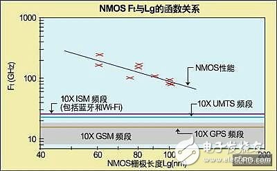
Figure 1: Tracking the cutoff frequency of each process node helps evaluate which communication bands can be processed in the digital domain.
Let’s look at the requirements for 3G mobile phones. In the digital domain, users expect higher-resolution displays, advanced gaming, PDA applications, and multimedia features like video calling and audio playback. On the RF side, integrating multiple radios into a single device is becoming increasingly common. These include GSM support across multiple bands, UMTS, GPS, Bluetooth, WiFi, Digital TV, and even FM broadcasting.
Today, over half of the components on a PCB are RF-related, and a single radio can occupy up to 40% of the board space. Adding more radios for Bluetooth, GPS, and WLAN only increases these numbers. While some circuits may be shared, the trend is clear: radios must become smaller to fit into compact devices.
Challenges in Integration
Integrating digital, analog, and RF circuits presents numerous practical challenges that have slowed down full-scale SoC adoption. Current EDA tools are still lacking in handling complex RF integration, especially when it comes to verification and testing. Other limitations include poor small-device matching, high 1/f noise, and the absence of sufficient on-chip passive components like resistors and capacitors.
Despite these obstacles, integration remains essential for reducing the cost, power consumption, and complexity of smartphone radios. To make this a reality, the industry needs breakthroughs in wafer fabrication, system architecture, and circuit design. Even though SoC designers may not directly deal with all these challenges, understanding them is crucial, as they shape the performance and capabilities of real-world devices.
For instance, while integrating RF using bipolar or BiCMOS processes is technically possible, the low yield and high testing costs make it unsuitable for mass production. Similarly, SiGe BiCMOS offers some benefits, but it lags behind advanced CMOS in terms of process nodes, making it less viable for memory-intensive mobile applications.
Even with CMOS, RF integration poses its own set of difficulties. Implementing analog components like mixers, filters, and amplifiers is challenging, especially with voltage drops and incomplete modeling for new process nodes. The industry needs innovative solutions that allow RF to be fully integrated into standard CMOS without compromising performance.
An alternative approach is to shift RF functionality entirely into the digital domain, effectively bypassing the challenges of analog RF design. By processing RF signals in the digital domain, there's no need for expensive analog masks, and chip design becomes simpler. Engineers can simulate and control signal processing more easily, leveraging programmable hardware and software elements for better flexibility.
For example, noise from the power supply can interfere with VCOs in RF circuits, affecting overall system efficiency. Traditional designs require regulators and passive components to mitigate this. However, integrating these into the transceiver reduces the need for external components, simplifying the design and saving space.
Designers can also integrate digital tuning and self-calibration into VCOs, along with loop filters, to extend their tuning range. This level of integration improves reliability and performance while keeping the design compact.
To process analog signals in digital circuits, the system must operate at extremely high speeds. The device’s cutoff frequency (Ft) is a key metric used to assess how well a process can handle RF signals. As shown in Figure 1, tracking this value across different process nodes helps determine which communication bands can be managed digitally.
12 Hour Timer Socket,24 Hour Timer Socket,24 hour digital timer plug,24 hour mechanical timer plug
NINGBO COWELL ELECTRONICS & TECHNOLOGY CO., LTD , https://www.cowellsocket.com